Comparative Analysis of Resistive RAM and DRAM Technologies
OCT 9, 20259 MIN READ
Generate Your Research Report Instantly with AI Agent
Patsnap Eureka helps you evaluate technical feasibility & market potential.
Memory Evolution and Research Objectives
Memory technologies have undergone significant evolution since the inception of computing systems. The journey began with magnetic core memory in the 1950s, which was subsequently replaced by semiconductor-based memory technologies. Dynamic Random Access Memory (DRAM) emerged in the late 1960s and has since dominated the main memory landscape due to its balance of density, speed, and cost-effectiveness. However, as Moore's Law approaches its physical limits, traditional DRAM scaling faces increasing challenges in terms of power consumption, reliability, and miniaturization potential.
Resistive RAM (ReRAM) represents one of the most promising emerging non-volatile memory technologies that could potentially complement or even replace DRAM in certain applications. Unlike DRAM, which stores information as electrical charges in capacitors requiring constant refreshing, ReRAM stores data by changing the resistance of a dielectric material, maintaining its state even when power is removed. This fundamental difference creates opportunities for addressing several limitations inherent to DRAM technology.
The current memory hierarchy faces significant challenges as the performance gap between processors and memory continues to widen, creating what is known as the "memory wall." DRAM's scaling limitations and power consumption issues have become increasingly problematic as computing systems demand higher bandwidth, lower latency, and improved energy efficiency. These challenges necessitate exploration of alternative memory technologies that can better meet the evolving requirements of modern computing paradigms.
This technical research aims to conduct a comprehensive comparative analysis between ReRAM and DRAM technologies across multiple dimensions including performance metrics, power efficiency, scalability, reliability, and integration potential. By examining the fundamental operating principles, architectural implications, and technological maturity of both memory types, we seek to identify the specific application domains where ReRAM might offer advantages over traditional DRAM solutions.
The research objectives include quantifying the performance trade-offs between these technologies under various workloads, evaluating their integration potential in existing memory hierarchies, and assessing the economic viability of ReRAM adoption in commercial systems. Additionally, we aim to identify the key technical hurdles that must be overcome for ReRAM to achieve mainstream adoption and explore potential hybrid memory architectures that leverage the complementary strengths of both technologies.
Through this analysis, we intend to provide strategic insights into the future memory landscape and establish a technological roadmap that guides research and development efforts in memory systems. The findings will inform decisions regarding investment priorities, partnership opportunities, and product development strategies in the rapidly evolving memory technology ecosystem.
Market Demand Analysis for Next-Generation Memory
The memory technology market is experiencing a significant shift driven by the increasing demands of data-intensive applications. Current projections indicate the global next-generation memory market will reach approximately $20 billion by 2026, with a compound annual growth rate exceeding 29%. This growth is primarily fueled by the limitations of conventional DRAM technology in meeting the requirements of emerging computing paradigms.
Data centers represent the largest market segment for advanced memory solutions, as they struggle with the memory wall problem where processing capabilities outpace memory performance. The exponential growth in cloud computing services has created unprecedented demand for memory technologies that can deliver higher bandwidth, lower latency, and improved power efficiency compared to traditional DRAM.
Mobile devices constitute another critical market segment, where battery life constraints make power-efficient memory solutions particularly valuable. Resistive RAM (ReRAM) shows promising characteristics in this domain, with potential power consumption reductions of 40-60% compared to conventional DRAM implementations in specific applications.
Artificial intelligence and machine learning applications have emerged as significant drivers for next-generation memory adoption. These workloads require massive parallel data access and high-bandwidth memory interfaces that traditional DRAM architectures struggle to provide efficiently. Industry analysts report that AI training and inference operations could benefit from ReRAM's non-volatile characteristics and potential for in-memory computing, potentially reducing energy consumption by 30-50% for specific neural network operations.
The automotive sector represents a rapidly growing market for advanced memory technologies, particularly with the rise of autonomous vehicles. These systems require memory solutions that can withstand extreme operating conditions while delivering real-time performance for sensor data processing. The automotive memory market segment is expected to grow at 34% annually through 2025, outpacing most other application areas.
Enterprise storage systems are increasingly adopting hybrid memory architectures that combine the strengths of different memory technologies. This trend is driving demand for solutions that can bridge the performance gap between DRAM and storage, with ReRAM positioned as a potential technology to address this middle ground in the memory hierarchy.
Geographic market distribution shows North America leading in adoption of next-generation memory technologies, followed by Asia-Pacific and Europe. China's significant investments in semiconductor independence are accelerating domestic development of alternative memory technologies, potentially reshaping the global market landscape over the next decade.
RRAM vs DRAM: Technical Challenges and Limitations
Despite their widespread adoption, both RRAM and DRAM technologies face significant technical challenges that limit their performance and broader application. DRAM's fundamental limitation stems from its volatile nature, requiring constant power to maintain stored data. This volatility necessitates periodic refresh operations, typically every 64ms, which consumes substantial power and creates performance bottlenecks in memory-intensive applications. Additionally, DRAM scaling faces physical barriers as cell sizes approach atomic dimensions, with current technologies struggling below 10nm node.
DRAM's charge-based storage mechanism becomes increasingly unreliable at smaller dimensions due to reduced capacitance and increased leakage currents. The capacitor's ability to maintain sufficient charge separation diminishes with size reduction, leading to higher error rates and more frequent refresh requirements. These scaling challenges have slowed DRAM's density improvements compared to historical trends, creating a growing gap between processor and memory performance.
RRAM, while promising as a non-volatile alternative, confronts its own set of technical hurdles. Endurance remains a critical limitation, with most commercial RRAM cells supporting 10^6 to 10^9 write cycles—significantly lower than DRAM's 10^15 cycles. This restricts RRAM's suitability for write-intensive applications like main memory. The resistance switching mechanism in RRAM also exhibits variability between cycles and between devices, complicating reliable multi-level cell implementation.
The forming process required to initialize RRAM cells introduces manufacturing complexity and potential reliability issues. Many RRAM technologies require relatively high operating voltages (2-5V) compared to DRAM (1.2V), creating integration challenges with advanced CMOS logic. Write latency for RRAM typically ranges from 10-100ns, slower than DRAM's 10-20ns, impacting system performance in write-intensive scenarios.
Material stability presents another significant challenge for RRAM. The filament formation and dissolution processes can lead to material migration and structural changes over time, potentially causing device degradation and failure. Temperature sensitivity affects both technologies differently—DRAM refresh rates must increase at higher temperatures due to accelerated charge leakage, while RRAM's resistance states can become less distinct at elevated temperatures.
Power consumption patterns differ substantially between the technologies. DRAM's dynamic power consumption is dominated by refresh operations, while RRAM's power profile is characterized by high write energy but negligible standby power. This fundamental difference creates distinct optimization challenges for system designers targeting different application scenarios.
Current Technical Solutions in Memory Architecture
01 Integration of Resistive RAM and DRAM technologies
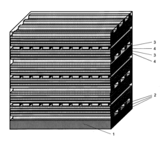
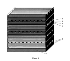
Various architectures and methods for integrating Resistive RAM (ReRAM) with Dynamic RAM (DRAM) technologies have been developed to leverage the advantages of both memory types. These hybrid memory systems combine the non-volatility and high density of ReRAM with the speed and established infrastructure of DRAM. Integration approaches include stacking memory layers, creating unified memory controllers, and developing compatible interface protocols that allow both memory types to coexist in computing systems.- Integration of RRAM and DRAM technologies: Integration of Resistive RAM (RRAM) and Dynamic RAM (DRAM) technologies in memory systems to leverage the advantages of both memory types. This approach combines the non-volatility and high density of RRAM with the speed and established infrastructure of DRAM. Such hybrid memory architectures can provide improved performance, power efficiency, and data persistence compared to traditional memory systems.
- Memory architecture and control systems: Specialized memory architecture and control systems designed to manage both RRAM and DRAM components efficiently. These systems include controllers that handle the different timing, voltage requirements, and access protocols of both memory types. The architecture may include shared data buses, address decoders, and signal conditioning circuits that enable seamless operation between the different memory technologies.
- Manufacturing processes for RRAM and DRAM integration: Manufacturing techniques and processes that enable the fabrication of integrated RRAM and DRAM components on the same chip or package. These processes address challenges such as material compatibility, thermal budgets, and process integration. Specialized fabrication methods may include novel deposition techniques, etching processes, and interconnect strategies to optimize the performance of both memory types while maintaining manufacturing efficiency.
- Power management in hybrid memory systems: Power management techniques specifically designed for hybrid RRAM-DRAM memory systems. These techniques leverage the non-volatile nature of RRAM to store data during low-power states while using DRAM for active operations. Advanced power control circuits can selectively power down memory sections not in use, implement variable refresh rates for DRAM components, and manage the different voltage requirements of each memory type to optimize overall system energy consumption.
- Data management and caching strategies: Specialized data management and caching strategies for systems incorporating both RRAM and DRAM. These strategies determine optimal data placement between the two memory types based on access patterns, data persistence requirements, and performance needs. Intelligent controllers can implement predictive algorithms to move data between RRAM and DRAM based on usage history, application requirements, and system state, maximizing the advantages of each memory technology.
02 Memory control and addressing mechanisms
Specialized control and addressing mechanisms have been developed to manage the different operational characteristics of Resistive RAM and DRAM in hybrid memory systems. These mechanisms include memory controllers that can handle different timing requirements, address mapping schemes that optimize data placement based on access patterns, and intelligent caching algorithms that determine which data should reside in which memory type. These control systems aim to maximize performance while managing the different write endurance and latency characteristics of each memory technology.Expand Specific Solutions03 Power management and non-volatile operation
Power management techniques specifically designed for hybrid Resistive RAM and DRAM systems leverage the non-volatile nature of ReRAM to reduce overall system power consumption. These techniques include power-down modes where data in volatile DRAM is transferred to non-volatile ReRAM during low-power states, fast wake-up mechanisms that restore system state from ReRAM, and dynamic power allocation based on workload characteristics. The non-volatile properties of ReRAM enable persistent memory applications while DRAM provides high-speed operation when the system is fully powered.Expand Specific Solutions04 Manufacturing and fabrication techniques
Advanced manufacturing and fabrication techniques have been developed to enable the production of integrated circuits containing both Resistive RAM and DRAM components. These techniques address challenges such as material compatibility, thermal budgets during processing, and interconnection strategies. Approaches include 3D stacking of memory layers, monolithic integration on the same silicon substrate, and the development of compatible materials and processes that allow both memory types to be manufactured using similar equipment and process flows.Expand Specific Solutions05 Performance optimization and memory hierarchy design
System architectures that optimize the performance of combined Resistive RAM and DRAM systems focus on creating effective memory hierarchies. These designs position DRAM as a faster cache or buffer for the larger, slower ReRAM storage layer. Techniques include predictive data movement algorithms that anticipate which data should be moved between memory types, specialized cache coherence protocols for hybrid memory systems, and application-specific optimizations that match memory characteristics to workload requirements. These approaches aim to deliver the speed of DRAM with the capacity and non-volatility of ReRAM.Expand Specific Solutions
Key Industry Players in Memory Semiconductor Market
The resistive RAM (ReRAM) and DRAM technology landscape is currently in a transitional phase, with ReRAM emerging as a promising non-volatile alternative to traditional memory solutions. The global memory market, valued at approximately $120 billion, shows DRAM dominating with mature manufacturing processes led by Samsung, SK Hynix, and Micron. Meanwhile, ReRAM technology is advancing through research and development efforts from companies like CrossBar, Adesto Technologies, and KIOXIA, though still in early commercialization stages. Major semiconductor manufacturers including TSMC, Intel, and IBM are investing in ReRAM research, recognizing its potential for lower power consumption and higher density storage. The competitive dynamics are shifting as foundries and memory specialists collaborate to overcome technical challenges in ReRAM scalability and endurance, positioning it as a complementary rather than replacement technology to DRAM in the near term.
Samsung Electronics Co., Ltd.
Technical Solution: Samsung has pioneered significant advancements in both DRAM and ReRAM technologies. For DRAM, Samsung has developed High Bandwidth Memory (HBM) solutions that stack multiple DRAM dies vertically with through-silicon vias (TSVs), achieving bandwidth up to 900 GB/s in their latest HBM3 offerings. Their DRAM technology incorporates 1y-nm class process technology with advanced cell structures to maintain capacitance while reducing cell area. For ReRAM, Samsung has developed cross-point array architectures that enable high-density storage with multi-level cell capabilities. Their ReRAM technology utilizes metal oxide switching materials (primarily hafnium oxide-based) that demonstrate reliable resistance switching characteristics with endurance exceeding 10^6 cycles. Samsung has also implemented innovative selector devices to minimize sneak path currents in high-density arrays, significantly improving read accuracy and energy efficiency.
Strengths: Samsung possesses comprehensive manufacturing infrastructure for both technologies, allowing seamless integration into existing product lines. Their vertical integration enables optimization across design, fabrication, and packaging. Weaknesses: Samsung's ReRAM solutions still face challenges in scaling to the same density levels as their DRAM products while maintaining competitive cost structures. Their ReRAM technology also requires higher operating voltages compared to DRAM, creating power management challenges in mobile applications.
Micron Technology, Inc.
Technical Solution: Micron has developed comprehensive solutions in both DRAM and ReRAM domains. Their DRAM technology features 1α nm process nodes with innovative capacitor designs that maintain charge storage capability while reducing cell size. Micron's DRAM implements advanced buried wordline architectures and optimized cell layouts that minimize interference between adjacent cells, enabling reliable operation at high densities. For ReRAM, Micron (particularly through their former subsidiary Qimonda) has developed conductive-bridging RAM (CBRAM) technology that utilizes electrochemical metallization cells. Their ReRAM architecture employs silver-based filament formation in a solid electrolyte, achieving switching speeds under 10ns and write energies below 0.1pJ per bit. Micron has also pioneered 3D crosspoint memory architecture (jointly with Intel as 3D XPoint) that combines elements of ReRAM technology to create high-density, non-volatile memory with DRAM-like performance characteristics. Their comparative analysis shows ReRAM achieving 1000x better endurance than NAND flash while offering 10x density advantage over DRAM.
Strengths: Micron's extensive experience in memory manufacturing enables efficient production scaling for both technologies. Their ReRAM solutions demonstrate superior endurance compared to other non-volatile memories while approaching DRAM performance metrics. Weaknesses: Their ReRAM technology still exhibits higher write latency compared to DRAM (typically 2-3x slower), limiting applications requiring frequent write operations. Cost-per-bit for their ReRAM solutions remains higher than DRAM, creating adoption barriers in price-sensitive markets.
Core Patents and Innovations in RRAM and DRAM
Strained Multilayer Resistive-Switching Memory Elements
PatentInactiveUS20160087196A1
Innovation
- A resistive-switching memory element comprising a plurality of metal oxide layers with neighboring layers having different lattice constants, creating strain that enhances resistance state retention and reduces read/write time, using electrodes made from conductive materials like noble metals and metal oxides, and deposited on flexible substrates for improved performance.
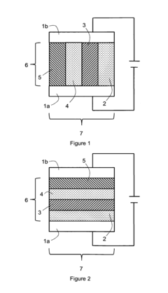
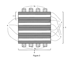
Resistive random access memory devices and resistive random access memory arrays having the same
PatentActiveUS8278640B2
Innovation
- The RRAM device incorporates a variable resistance material layer made of metallic oxide with an intermediate electrode layer of low oxygen reactivity, such as indium tin oxide (ITO), and a second electrode layer with a higher or lower work function than tantalum (Ta) to maintain oxygen regions and achieve multi-level resistance states without requiring high voltage programming.
Power Efficiency and Sustainability Considerations
Power efficiency has emerged as a critical factor in memory technology evaluation, particularly when comparing Resistive RAM (ReRAM) and Dynamic RAM (DRAM). ReRAM demonstrates significant advantages in static power consumption, requiring virtually no power to maintain stored data, unlike DRAM which necessitates constant refresh cycles to preserve information. This fundamental architectural difference results in ReRAM consuming approximately 10-20 times less standby power than conventional DRAM systems.
During active operations, ReRAM continues to demonstrate superior efficiency metrics. Write operations in ReRAM typically consume 0.1-1 pJ/bit compared to DRAM's 2-5 pJ/bit, representing a substantial energy reduction. Read operations show similar advantages, with ReRAM requiring approximately 0.1-0.5 pJ/bit versus 1-3 pJ/bit for DRAM. These efficiency gains become particularly significant in data-intensive applications where memory operations constitute a substantial portion of system power consumption.
From a sustainability perspective, ReRAM offers several environmental advantages. The reduced power requirements directly translate to lower carbon emissions during operation, an increasingly important consideration as data centers expand globally. Additionally, ReRAM's non-volatile nature enables more aggressive power management strategies, allowing systems to completely power down memory components during idle periods without data loss.
Manufacturing sustainability also favors ReRAM in several aspects. The fabrication process for ReRAM typically requires fewer processing steps and potentially uses less toxic materials compared to DRAM production. Furthermore, ReRAM's simpler cell structure may reduce resource requirements and manufacturing waste. Recent life cycle assessments suggest ReRAM could reduce the environmental impact of memory production by 15-30% compared to equivalent DRAM capacity.
The longevity factor presents a more complex picture. While ReRAM offers superior endurance to flash memory (10^6-10^9 write cycles versus 10^4-10^5), it still falls short of DRAM's practically unlimited write endurance. However, ReRAM's longer operational lifespan in low-power applications may offset this limitation by reducing replacement frequency and associated electronic waste.
As energy costs and environmental regulations become increasingly stringent, ReRAM's efficiency advantages position it favorably for future computing systems. Data centers, edge computing devices, and IoT applications stand to benefit significantly from ReRAM's reduced power profile. Industry projections suggest that widespread ReRAM adoption could reduce global data center energy consumption by 3-7% by 2030, representing both substantial cost savings and environmental benefits.
Integration Pathways for Hybrid Memory Systems
The integration of Resistive RAM (ReRAM) and DRAM technologies into hybrid memory systems represents a significant advancement in memory architecture design. These integration pathways can be categorized into three primary approaches: vertical integration, horizontal integration, and hierarchical integration, each offering distinct advantages for specific application scenarios.
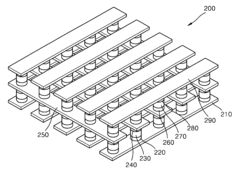
Vertical integration involves stacking ReRAM and DRAM layers in a 3D configuration, maximizing density while minimizing footprint. This approach has gained traction with the development of through-silicon via (TSV) technology, which enables high-bandwidth connections between memory layers. Companies like Samsung and SK Hynix have demonstrated prototypes achieving up to 4x higher density compared to traditional 2D implementations, while maintaining acceptable latency characteristics.
Horizontal integration places ReRAM and DRAM modules side-by-side on the same die or package, connected through high-speed interconnects. This configuration allows for independent optimization of each memory type while maintaining relatively low communication latency between them. Intel's Optane DC Persistent Memory represents a commercial implementation of this approach, pairing DRAM with non-volatile memory on the same memory channel.
Hierarchical integration implements ReRAM and DRAM at different levels of the memory hierarchy, with DRAM typically serving as a cache or buffer for the ReRAM. This approach leverages the speed of DRAM for frequently accessed data while utilizing ReRAM's non-volatility and density for bulk storage. IBM's Memory-Centric Computing architecture exemplifies this strategy, demonstrating up to 40% reduction in overall system power consumption.
The controller architecture plays a crucial role in hybrid memory systems, requiring sophisticated algorithms for data placement, migration, and coherence management. Recent advances in machine learning-based memory controllers have shown promise in predicting access patterns and optimizing data placement dynamically, reducing the performance gap between ReRAM and DRAM by up to 30% in benchmark tests.
Software support remains a significant challenge, with operating systems and applications requiring modifications to fully exploit hybrid memory capabilities. Memory-aware programming models like Persistent Memory Development Kit (PMDK) are emerging to address this gap, providing developers with tools to effectively utilize heterogeneous memory resources.
Looking forward, chiplet-based integration approaches are gaining momentum, allowing for more flexible combinations of memory technologies with reduced manufacturing complexity. This modular approach enables system designers to tailor memory configurations to specific workload requirements while maintaining economic viability through standardized interfaces.
Unlock deeper insights with Patsnap Eureka Quick Research — get a full tech report to explore trends and direct your research. Try now!
Generate Your Research Report Instantly with AI Agent
Supercharge your innovation with Patsnap Eureka AI Agent Platform!