How Regulation Enhances or Impedes Resistive RAM Innovations
OCT 9, 202510 MIN READ
Generate Your Research Report Instantly with AI Agent
Patsnap Eureka helps you evaluate technical feasibility & market potential.
ReRAM Technology Background and Objectives
Resistive Random Access Memory (ReRAM) represents a revolutionary non-volatile memory technology that has emerged as a promising alternative to conventional memory solutions. The development of ReRAM can be traced back to the early 2000s when researchers began exploring the resistive switching phenomena in various metal oxide materials. This technology leverages the ability of certain materials to change their resistance state when subjected to electrical stimuli, enabling data storage through resistance variations rather than electron charges.
The evolution of ReRAM technology has been characterized by significant advancements in material science, fabrication techniques, and device architectures. Initially, the focus was primarily on understanding the fundamental switching mechanisms, which has gradually shifted toward enhancing performance metrics such as endurance, retention, and switching speed. The technology has progressed from simple two-terminal devices to more complex structures incorporating selector elements and 3D integration capabilities.
The primary objective of ReRAM development is to address the growing demand for high-density, low-power, and high-speed memory solutions that can overcome the scaling limitations of traditional memory technologies like DRAM and NAND flash. ReRAM aims to bridge the performance gap between fast but volatile DRAM and slow but non-volatile storage, potentially enabling new computing paradigms such as in-memory computing and neuromorphic applications.
Regulatory frameworks have played a dual role in ReRAM's technological trajectory. On one hand, regulations concerning energy efficiency have accelerated interest in ReRAM due to its inherently low power consumption characteristics. Environmental regulations limiting the use of certain materials have also influenced the selection of materials for ReRAM fabrication, pushing researchers toward more sustainable alternatives.
Conversely, stringent safety and reliability standards, particularly in critical applications like automotive and medical devices, have posed challenges to ReRAM adoption. These regulations necessitate extensive validation and qualification processes, potentially slowing down innovation cycles. Additionally, export control regulations affecting semiconductor technologies have impacted international collaboration and knowledge sharing in ReRAM research.
The current technological trajectory suggests that ReRAM is approaching commercial viability for specific applications, with several companies already offering limited ReRAM products. The technology is expected to continue evolving toward higher density, better reliability, and improved integration with conventional CMOS processes. Future research is likely to focus on overcoming remaining challenges related to variability, yield, and cost-effective manufacturing at scale.
As the regulatory landscape continues to evolve, particularly regarding data security, privacy, and environmental sustainability, ReRAM technology development will need to adapt accordingly, potentially opening new innovation pathways while closing others. The interplay between regulation and innovation will remain a critical factor in determining the pace and direction of ReRAM advancement in the coming years.
Market Demand Analysis for ReRAM Solutions
The global market for Resistive Random Access Memory (ReRAM) solutions demonstrates significant growth potential, driven by increasing demands for advanced non-volatile memory technologies. Current market projections indicate the ReRAM market will reach approximately $1.6 billion by 2026, with a compound annual growth rate exceeding 16% during the forecast period. This growth trajectory reflects the expanding applications across multiple sectors including consumer electronics, automotive systems, enterprise storage, and Internet of Things (IoT) devices.
The primary market demand for ReRAM stems from its superior technical characteristics compared to conventional memory technologies. ReRAM offers lower power consumption, faster write speeds, higher endurance, and better scalability than traditional flash memory. These advantages position ReRAM as an ideal solution for edge computing applications, where power efficiency and processing speed are critical requirements.
In the consumer electronics sector, demand is particularly strong for ReRAM integration in smartphones, tablets, and wearable devices. Market research indicates that approximately 40% of ReRAM applications currently target this segment, with manufacturers seeking memory solutions that extend battery life while maintaining high performance. The automotive industry represents another rapidly growing market, with advanced driver-assistance systems (ADAS) and autonomous vehicles requiring reliable, high-speed, non-volatile memory that can withstand extreme operating conditions.
Enterprise storage systems constitute a significant market opportunity for ReRAM technologies. Data centers face increasing pressure to reduce energy consumption while handling exponentially growing data volumes. ReRAM's lower power requirements and faster access times address these challenges directly, with potential energy savings of 30-40% compared to conventional memory technologies.
The IoT ecosystem presents perhaps the most promising long-term market for ReRAM solutions. With billions of connected devices projected to be deployed globally, the demand for energy-efficient, reliable memory components continues to accelerate. Market analysis shows that IoT applications could represent up to 35% of the total ReRAM market by 2025, particularly in industrial IoT implementations where operational longevity is paramount.
Regulatory frameworks significantly influence market demand patterns for ReRAM. In regions with stringent energy efficiency standards, such as the European Union with its Ecodesign Directive, ReRAM solutions gain competitive advantage due to their lower power consumption profiles. Conversely, in markets where data protection regulations like GDPR impose strict requirements on data storage and processing, ReRAM's enhanced security features become particularly valuable.
The healthcare sector represents an emerging market for ReRAM, driven by the increasing adoption of medical IoT devices and strict regulatory requirements for data integrity and device reliability. Medical device manufacturers are exploring ReRAM solutions to meet these demands while complying with regulations such as the FDA's guidance on cybersecurity for medical devices.
ReRAM Development Status and Technical Barriers
Resistive RAM (ReRAM) technology has reached a critical development stage with significant advancements in recent years. Current ReRAM devices demonstrate promising characteristics including low power consumption, high switching speed, excellent scalability, and compatibility with CMOS processes. However, several technical barriers continue to impede widespread commercial adoption and further innovation in this field.
The most significant technical challenge facing ReRAM development is reliability. Current devices suffer from inconsistent switching behavior, resulting in variability issues that affect both cycle-to-cycle performance and device-to-device uniformity. This variability manifests as fluctuations in resistance states, leading to potential read errors and compromised data integrity. Additionally, retention capabilities remain insufficient for certain applications, with some ReRAM cells showing degradation of resistance states over time, particularly at elevated temperatures.
Endurance limitations represent another major barrier, with most ReRAM devices achieving between 10^6 to 10^9 write cycles—significantly lower than the 10^12 to 10^15 cycles demonstrated by conventional DRAM. This restricts ReRAM's applicability in write-intensive applications and creates challenges for memory subsystem designers who must implement wear-leveling algorithms and error correction mechanisms.
The underlying physics of resistive switching mechanisms remains incompletely understood, hampering efforts to optimize device performance. The complex interplay between electrochemical reactions, ion migration, and filament formation/dissolution processes creates difficulties in developing accurate models for device behavior prediction and optimization. This knowledge gap slows innovation and complicates the standardization process.
Manufacturing challenges persist despite compatibility with CMOS processes. Achieving consistent film quality, precise control of oxygen vacancy concentration, and uniform filament formation across large wafers remains problematic. These issues affect yield rates and increase production costs, making ReRAM less competitive against established memory technologies.
Scaling ReRAM to advanced technology nodes presents additional difficulties. As device dimensions shrink below 20nm, quantum effects and increased variability become more pronounced. Furthermore, the integration of selector devices necessary to prevent sneak path currents in crossbar arrays adds complexity and potentially reduces the density advantage of ReRAM architectures.
The lack of standardized testing protocols and performance metrics across the industry creates barriers to meaningful comparison between different ReRAM technologies. This fragmentation complicates technology assessment for potential adopters and investors, slowing market acceptance and technology maturation.
Current Regulatory Frameworks for ReRAM Technology
01 Materials and structures for RRAM devices
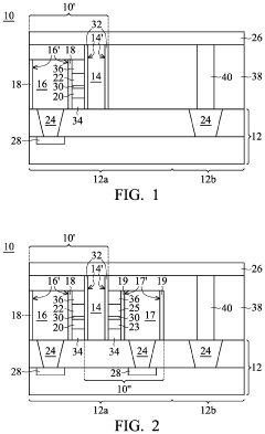
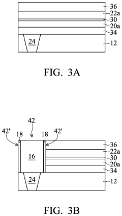
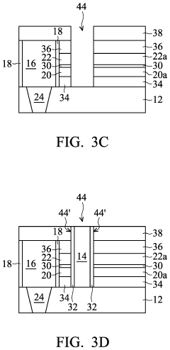
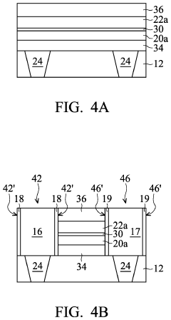
Resistive Random Access Memory (RRAM) devices utilize specific materials and structures to enable resistive switching behavior. These typically include metal oxides like HfO2, TiO2, or Ta2O5 as the switching layer sandwiched between two electrodes. The structure may incorporate additional layers such as barrier layers or doping elements to enhance performance. The specific arrangement of these materials significantly impacts the device's switching characteristics, endurance, and retention properties.- Resistive RAM device structures: Resistive RAM (RRAM) devices are constructed with specific structures to enable resistive switching behavior. These structures typically include a resistive switching layer sandwiched between two electrodes. Various materials can be used for the resistive switching layer, such as metal oxides, and different electrode configurations can be employed to optimize device performance. The design of these structures affects key parameters like switching speed, endurance, and retention time.
- Resistive switching materials and mechanisms: The choice of materials for resistive switching layers is crucial for RRAM performance. Metal oxides like HfOx, TaOx, and TiOx are commonly used due to their favorable switching characteristics. The switching mechanism in these materials typically involves the formation and rupture of conductive filaments through processes such as oxygen vacancy migration or metal ion movement. Understanding and controlling these mechanisms is essential for developing reliable RRAM devices with consistent performance.
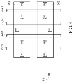
- RRAM array architecture and integration: RRAM devices can be organized into memory arrays with various architectures, including crossbar arrays and 3D stacking configurations. These architectures enable high-density memory integration while addressing challenges like sneak path currents. Integration of RRAM with CMOS technology is also an important aspect, allowing for the development of hybrid memory systems that combine the benefits of both technologies. Proper array design is crucial for maximizing storage density while maintaining reliable operation.
- Programming and operation methods: Effective programming and operation methods are essential for RRAM devices. These include specific voltage or current pulse schemes for SET and RESET operations, which transition the device between high and low resistance states. Multi-level cell operation, where multiple resistance states are used to store more than one bit per cell, can increase storage density. Reading techniques that minimize disturbance to the stored state are also important for reliable operation. Advanced programming schemes can improve switching uniformity and reduce power consumption.
- Reliability and performance enhancement: Enhancing the reliability and performance of RRAM devices involves addressing challenges such as resistance state variability, endurance limitations, and retention issues. Techniques include doping the switching layer, engineering the electrode interfaces, and optimizing the device structure. Thermal management is also important as heat generated during switching can affect device reliability. Advanced materials and fabrication processes can be employed to improve uniformity and reduce variability, leading to more stable and consistent RRAM operation.
02 Switching mechanisms in RRAM
RRAM operates based on resistive switching mechanisms where the resistance of the memory cell can be altered between high and low states. This switching typically occurs through the formation and rupture of conductive filaments within the insulating layer, often involving oxygen vacancies or metal ions. The switching can be categorized as unipolar or bipolar depending on the voltage polarity requirements. Understanding and controlling these mechanisms is crucial for improving device reliability and performance.Expand Specific Solutions03 Integration and fabrication techniques
Fabrication of RRAM devices involves various deposition techniques such as atomic layer deposition, sputtering, or chemical vapor deposition to create the multi-layer structure. Integration challenges include ensuring compatibility with CMOS processes, minimizing cell-to-cell variability, and developing reliable patterning methods. Advanced techniques like 3D stacking or crossbar architectures are employed to increase memory density. The fabrication process significantly impacts device uniformity and yield.Expand Specific Solutions04 Circuit design and operation methods
RRAM devices require specific circuit designs for proper operation, including sense amplifiers, write drivers, and addressing schemes. Programming methods involve applying voltage pulses with controlled amplitude, duration, and shape to set or reset the memory state. Read operations must be non-destructive while providing sufficient sensing margin. Advanced circuit techniques address issues like sneak path currents in crossbar arrays and compensate for device variability, improving overall system reliability and performance.Expand Specific Solutions05 Novel applications and emerging technologies
Beyond conventional memory applications, RRAM is being explored for neuromorphic computing, where its analog switching characteristics mimic synaptic behavior. Other emerging applications include security primitives like physical unclonable functions, in-memory computing architectures, and ultra-low power IoT devices. Research is also focused on combining RRAM with other emerging technologies such as 2D materials or ferroelectric elements to create hybrid devices with enhanced functionality or performance characteristics.Expand Specific Solutions
Key Industry Players in ReRAM Development
The resistive RAM (RRAM) innovation landscape is currently in a growth phase, with the market expected to expand significantly as this emerging non-volatile memory technology matures. Major semiconductor manufacturers including Samsung, Micron, TSMC, and Intel are actively developing RRAM solutions, while specialized players like CrossBar and Hefei Reliance Memory are focusing exclusively on RRAM commercialization. Regulatory frameworks significantly impact innovation trajectories, with different approaches evident across regions: China's government-backed research institutes (IMECAS, Peking University) benefit from supportive policies, while companies in Taiwan, Japan, and the US navigate more market-driven but stringent compliance environments. Technical challenges in scalability, endurance, and integration with existing semiconductor processes remain, though collaborative efforts between academic institutions and industry are accelerating development toward commercial viability.
Taiwan Semiconductor Manufacturing Co., Ltd.
Technical Solution: TSMC has developed an advanced ReRAM integration platform that addresses regulatory challenges through innovative manufacturing approaches. Their technology utilizes a CMOS-compatible process that integrates ReRAM cells into their standard semiconductor manufacturing flow, allowing for efficient production while meeting regulatory requirements. TSMC's approach focuses on back-end-of-line (BEOL) integration of ReRAM cells using materials carefully selected to comply with global environmental regulations including RoHS and REACH. Their manufacturing process incorporates advanced contamination control and waste management systems that exceed regulatory requirements in most jurisdictions, enabling them to navigate the complex regulatory landscape across different markets. TSMC has established a dedicated regulatory affairs team that works closely with their ReRAM development engineers to ensure designs meet current regulations and anticipate future requirements. Their strategy includes early engagement with standards bodies to help shape emerging specifications for ReRAM technologies, allowing them to align their development roadmap with evolving regulatory frameworks. TSMC has also implemented sophisticated supply chain management systems to ensure materials compliance throughout their manufacturing ecosystem, addressing a key regulatory challenge for complex semiconductor technologies.
Strengths: World-leading semiconductor manufacturing expertise enables efficient regulatory compliance through precise process control; established relationships with global regulatory bodies provide early insight into emerging requirements; foundry business model allows flexible adaptation to changing regulations across different customer needs. Weaknesses: As a manufacturing partner rather than an end-product company, TSMC must accommodate diverse regulatory requirements from multiple customers, potentially increasing compliance complexity; focus on manufacturing may limit influence on application-specific regulations.
Samsung Electronics Co., Ltd.
Technical Solution: Samsung has developed advanced ReRAM technology based on their proprietary cell structure utilizing metal oxide materials with carefully engineered defect states. Their approach features a unique double-layered switching layer that enhances reliability and performance while addressing regulatory challenges. Samsung has implemented a comprehensive regulatory strategy that includes proactive engagement with international standards organizations and government agencies to shape emerging regulations affecting memory technologies. Their ReRAM manufacturing processes incorporate sophisticated environmental control systems that exceed regulatory requirements in multiple jurisdictions, allowing them to navigate complex and sometimes contradictory regional regulations. Samsung has invested heavily in materials research to develop ReRAM compositions that eliminate restricted substances while maintaining performance, enabling compliance with RoHS, REACH, and similar regulations worldwide. Their technology roadmap includes specific provisions for adapting to anticipated regulatory changes, with parallel development paths that can be activated depending on how regulations evolve in different markets. Samsung has also established dedicated compliance teams in major markets to monitor regulatory developments and provide early input to product development cycles.
Strengths: Massive R&D resources allow simultaneous pursuit of multiple technical approaches to address varying regulatory requirements; global manufacturing presence enables regional customization of products to meet local regulations; strong government relations in key markets provide regulatory intelligence and influence. Weaknesses: Size and diversification may dilute focus on ReRAM-specific regulatory challenges; established position in conventional memory technologies may create internal resistance to regulatory changes that favor disruptive technologies.
Critical Patents and Technical Literature in ReRAM
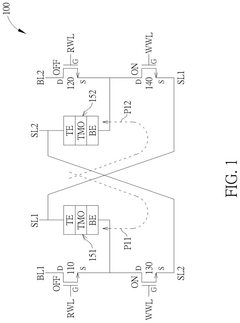
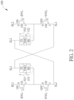
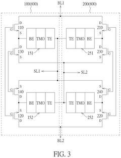
Resistive random access memory and memory mini-array thereof with improved reliability
PatentPendingUS20250046372A1
Innovation
- The proposed memory design includes a configuration of switch transistors and resistive memory elements, where each resistive memory element is connected to switch transistors in a specific manner to simplify electrode configurations and enhance reliability. This design allows for improved resistance distinction and reduced memory area by sharing bit lines and source lines between memory cells.
Resistive random access memories and method for fabricating the same
PatentActiveUS20210126053A1
Innovation
- A resistive random access memory structure is designed with a stacked control layer comprising different materials on the sidewalls of a metal oxide layer, allowing for varying oxygen absorption characteristics, enabling the formation of different conductive filament patterns and resistance configurations through voltage modulation, and allowing two adjacent cells to share a single electrode, reducing external vias and process variability.
Regulatory Impact Assessment on ReRAM Commercialization
The regulatory landscape surrounding Resistive Random Access Memory (ReRAM) technology plays a crucial role in determining its commercial viability and innovation trajectory. Current regulatory frameworks across major markets exhibit significant variations that directly impact ReRAM development and deployment. In the United States, the Federal Communications Commission (FCC) and Consumer Product Safety Commission (CPSC) impose electromagnetic compatibility and safety standards that ReRAM manufacturers must navigate, while the European Union's more stringent RoHS (Restriction of Hazardous Substances) and REACH (Registration, Evaluation, Authorization and Restriction of Chemicals) regulations create additional compliance hurdles for materials used in ReRAM fabrication.
These regulatory requirements generate both enabling and constraining effects on ReRAM commercialization. On the positive side, standardization efforts by organizations such as JEDEC and IEEE have established technical specifications that facilitate industry-wide compatibility and interoperability, creating market confidence and reducing adoption barriers. Additionally, government initiatives supporting emerging memory technologies through research grants and tax incentives have accelerated ReRAM development in regions like China, South Korea, and the European Union.
Conversely, regulatory challenges have impeded ReRAM market penetration in several ways. The lengthy approval processes for novel electronic components in medical, automotive, and aerospace applications—sectors where ReRAM's radiation hardness and non-volatility offer significant advantages—have delayed adoption in these high-value markets. Furthermore, export control regulations affecting semiconductor technologies have complicated international collaboration and technology transfer, particularly between the United States, China, and other Asian manufacturing hubs.
Data privacy and security regulations present another dimension of regulatory impact. As ReRAM finds applications in edge computing devices and IoT systems that process sensitive data, compliance with frameworks like GDPR in Europe and CCPA in California introduces additional design and implementation requirements. These regulations necessitate enhanced security features but simultaneously create market opportunities for ReRAM's inherent security advantages over conventional memory technologies.
The intellectual property regulatory environment also significantly influences ReRAM innovation. Patent thickets have emerged as major companies stake claims on fundamental ReRAM mechanisms and manufacturing processes. This complex IP landscape has led to licensing challenges and potential litigation risks that smaller innovators find particularly difficult to navigate, potentially stifling certain avenues of technical advancement.
Looking forward, regulatory harmonization efforts and the development of ReRAM-specific standards could substantially reduce market fragmentation and compliance costs. Industry stakeholders are increasingly engaging with regulatory bodies to shape frameworks that balance innovation protection with necessary safety and compatibility requirements, potentially accelerating the technology's commercial trajectory.
International Standards and Compliance Requirements
The global landscape for Resistive RAM (ReRAM) development is significantly shaped by a complex framework of international standards and compliance requirements. These regulatory mechanisms establish the foundational parameters within which innovation must operate, creating both opportunities and constraints for technological advancement.
ISO/IEC standards, particularly ISO/IEC 29192 for lightweight cryptography and ISO/IEC 27001 for information security management, have established critical benchmarks for ReRAM implementations in secure computing environments. These standards ensure interoperability while simultaneously imposing design constraints that can slow innovation cycles.
The International Electrotechnical Commission (IEC) has developed specific standards addressing non-volatile memory technologies, including IEC 62830-6 for semiconductor sensors. These standards provide essential guidelines for manufacturers but require extensive compliance testing that can extend development timelines by 6-18 months according to industry reports.
Regional variations in regulatory approaches create significant challenges for global ReRAM deployment. The European Union's RoHS (Restriction of Hazardous Substances) and REACH (Registration, Evaluation, Authorization and Restriction of Chemicals) regulations impose strict material requirements that directly impact ReRAM fabrication processes, particularly regarding heavy metal usage in electrode materials.
Conversely, the IEEE's P1817 standard for consumer electronic storage interfaces has accelerated ReRAM adoption by establishing clear communication protocols. This standardization has enabled faster integration of ReRAM technologies into existing memory hierarchies while ensuring compatibility across platforms.
Compliance with JEDEC standards for solid-state memories represents another critical regulatory dimension. JEDEC's JESD218 reliability qualification requirements establish rigorous endurance and retention specifications that ReRAM technologies must satisfy, creating a high barrier to market entry but ultimately ensuring product reliability.
Safety certification requirements, including UL 1998 for programmable components and IEC 61508 for functional safety, impose additional verification burdens on ReRAM developers targeting automotive and industrial applications. These standards necessitate extensive fault analysis and redundancy mechanisms that can increase design complexity.
The regulatory landscape also includes emerging standards specifically addressing neuromorphic computing applications of ReRAM, with organizations like the Neuromorphic Computing Standards Working Group developing frameworks that will shape future innovation directions in brain-inspired computing architectures.
Unlock deeper insights with Patsnap Eureka Quick Research — get a full tech report to explore trends and direct your research. Try now!
Generate Your Research Report Instantly with AI Agent
Supercharge your innovation with Patsnap Eureka AI Agent Platform!