

VCSEL Array Packaging For Co-Packaged Optics Applications
AUG 27, 202510 MIN READ
Generate Your Research Report Instantly with AI Agent
PatSnap Eureka helps you evaluate technical feasibility & market potential.
VCSEL Array Packaging Background and Objectives
Vertical-Cavity Surface-Emitting Laser (VCSEL) technology has evolved significantly since its inception in the late 1970s, with commercial availability beginning in the 1990s. The technology has progressed from single-element devices to sophisticated array configurations capable of high-speed data transmission. This evolution has been driven by increasing demands for higher bandwidth, lower power consumption, and more compact optical interconnect solutions in data centers and high-performance computing environments.
The emergence of co-packaged optics (CPO) represents a paradigm shift in optical interconnect architecture, where optical components are integrated directly with electronic devices such as ASICs or switch ICs. This approach addresses fundamental limitations in traditional pluggable optics by reducing signal path lengths, minimizing power consumption, and enabling higher bandwidth density. VCSEL arrays are particularly well-suited for CPO applications due to their compact size, low power requirements, and compatibility with silicon photonics platforms.
Current VCSEL array packaging technologies face significant challenges when adapted for CPO applications. Traditional packaging approaches often fail to meet the stringent thermal management requirements, alignment precision, and manufacturing scalability needed for effective integration with electronic components. The thermal interface between VCSELs and electronic components is particularly critical, as VCSEL performance is highly temperature-dependent.
The primary objective of VCSEL array packaging development for CPO applications is to create packaging solutions that enable seamless integration with electronic components while maintaining optimal optical performance. This includes achieving sub-micron alignment precision, effective thermal management to maintain wavelength stability, and compatibility with high-volume manufacturing processes to ensure cost-effectiveness.
Additional technical goals include reducing the form factor of packaged VCSEL arrays to accommodate dense integration requirements, developing hermetic sealing techniques compatible with silicon photonics platforms, and ensuring long-term reliability under varying operating conditions. The packaging solution must also address electrical interconnect challenges, providing low-impedance, high-bandwidth connections between the VCSEL array and driving electronics.
From an industry perspective, standardization of VCSEL array packaging for CPO applications remains a critical objective. Organizations such as the Optical Internetworking Forum (OIF) and IEEE are working to establish standards that will facilitate interoperability and accelerate market adoption. These standards aim to define common interfaces, performance metrics, and testing methodologies specific to CPO applications.
The development trajectory for VCSEL array packaging technology is expected to follow an evolutionary path, with incremental improvements in thermal management, alignment precision, and manufacturing techniques leading to revolutionary changes in optical interconnect architectures. The ultimate goal is to enable terabit-scale optical interconnects that can meet the exponentially growing bandwidth demands of next-generation computing and communication systems.
Market Demand Analysis for Co-Packaged Optics
The co-packaged optics (CPO) market is experiencing significant growth driven by the increasing demand for high-bandwidth, energy-efficient data center interconnects. As data centers scale to meet the exponential growth in cloud computing, artificial intelligence, and 5G applications, traditional pluggable optics face fundamental limitations in power consumption and density. This market shift has created substantial opportunities for VCSEL array packaging technologies specifically designed for CPO applications.
Current market analysis indicates that the global CPO market is projected to grow at a compound annual growth rate of over 26% from 2023 to 2028. This growth is primarily fueled by hyperscale data center operators seeking to overcome the "bandwidth wall" while simultaneously addressing power efficiency concerns. The market demand is particularly strong in North America and Asia-Pacific regions, where major cloud service providers are aggressively expanding their infrastructure.
From an application perspective, the demand for CPO solutions is most pronounced in high-performance computing environments, AI/ML training clusters, and next-generation data center architectures. These applications require data rates exceeding 800G and moving toward 1.6T and 3.2T, which conventional pluggable optics struggle to support efficiently. VCSEL array packaging for CPO addresses these needs by enabling shorter optical paths, reduced power consumption, and higher integration density.
Industry surveys reveal that power efficiency is the primary driver for CPO adoption, with data center operators reporting that traditional pluggable optics can consume up to 30% of their total power budget. By integrating optical components directly with switch ASICs, CPO solutions can potentially reduce power consumption by 25-40%, representing significant operational cost savings for large-scale deployments.
The market is also witnessing increasing demand for standardization in CPO interfaces. Organizations such as the Open Compute Project (OCP) and Consortium for On-Board Optics (COBO) are actively developing specifications to ensure interoperability across different vendors' solutions. This standardization effort is expected to accelerate market adoption by reducing implementation risks and ensuring long-term investment protection.
Supply chain considerations are becoming increasingly important in the CPO market. Recent global semiconductor shortages have highlighted the vulnerability of complex technology supply chains. Consequently, data center operators are placing greater emphasis on supply chain resilience when evaluating CPO solutions, creating opportunities for VCSEL array packaging technologies that can be manufactured through diversified supply chains.
Looking at customer segments, while hyperscale cloud providers currently represent the largest market for CPO solutions, there is growing interest from telecommunications providers and enterprise data centers. This broadening customer base suggests that VCSEL array packaging for CPO applications has potential beyond its initial target market, indicating robust long-term growth prospects.
VCSEL Packaging Technical Challenges and Constraints
VCSEL array packaging for co-packaged optics applications faces several significant technical challenges that must be addressed to ensure optimal performance and reliability. The primary constraint lies in the thermal management of these densely packed arrays. VCSELs generate substantial heat during operation, and without effective thermal dissipation, their performance degrades rapidly, leading to wavelength shifts, reduced output power, and shortened device lifetime. This challenge is particularly acute in co-packaged optics where multiple VCSELs operate in close proximity.
Alignment precision represents another critical constraint. VCSEL arrays require sub-micron alignment accuracy between the emitter and coupling optics to maintain optical efficiency. This precision must be maintained throughout the device's operational lifetime despite thermal cycling and mechanical stresses, necessitating advanced packaging techniques that can preserve alignment integrity under varying environmental conditions.
The electrical interconnection design presents significant challenges, particularly as data rates increase. High-frequency signal integrity must be maintained while minimizing crosstalk between channels. This requires careful consideration of transmission line effects, impedance matching, and signal routing within the package. Additionally, the electrical interfaces must accommodate the high current densities required for VCSEL operation without compromising reliability.
Hermeticity and environmental protection constitute another major constraint. VCSELs are sensitive to moisture and contaminants, which can cause catastrophic failures through mechanisms such as oxidation or corrosion. Packaging solutions must provide effective barriers against these environmental factors while still allowing for efficient optical coupling and thermal management.
Manufacturing scalability presents a significant challenge for widespread adoption. Current high-precision packaging techniques often involve labor-intensive processes that are difficult to scale for high-volume production. The industry needs packaging approaches that can be automated while maintaining the required precision and reliability.
Size constraints are particularly demanding in co-packaged optics applications. The packaging solution must minimize footprint and profile while accommodating all necessary functional elements including thermal management structures, electrical interconnects, and optical coupling components. This spatial limitation often forces difficult design trade-offs between performance parameters.
Cost effectiveness remains a persistent constraint. Despite the technical complexities involved, VCSEL array packages must meet aggressive price targets to enable mass adoption in data center and telecommunications applications. This necessitates innovations in materials, processes, and design that can reduce manufacturing costs without compromising essential performance characteristics.
Current VCSEL Array Packaging Solutions
01 Thermal Management Solutions for VCSEL Arrays
Effective thermal management is critical for VCSEL array packaging to ensure optimal performance and longevity. Various solutions include integrating heat sinks, thermal interface materials, and specialized substrates that efficiently dissipate heat generated during operation. These thermal management techniques help maintain stable operating temperatures, prevent thermal runaway, and ensure consistent optical output across the array elements.- Thermal Management in VCSEL Array Packaging: Effective thermal management is crucial in VCSEL array packaging to ensure optimal performance and longevity. Various techniques are employed to dissipate heat generated during operation, including the use of specialized heat sinks, thermally conductive materials, and strategic package designs. These approaches help maintain stable operating temperatures, prevent thermal runaway, and ensure consistent optical output across the array elements.
- Optical Alignment and Coupling Solutions: Precise optical alignment is essential in VCSEL array packaging to maximize light output efficiency and beam quality. This involves aligning the VCSEL array with optical elements such as lenses, waveguides, or optical fibers. Advanced packaging techniques incorporate passive alignment features, active alignment processes, and specialized coupling structures to ensure optimal light collection and transmission while maintaining the integrity of the optical characteristics.
- Hermetic Sealing and Environmental Protection: VCSEL arrays require protection from environmental factors such as moisture, dust, and contaminants that can degrade performance. Packaging solutions incorporate hermetic sealing techniques, specialized encapsulation materials, and protective coatings to ensure long-term reliability. These protective measures prevent oxidation of sensitive surfaces, maintain stable operating conditions, and extend the operational lifetime of the devices.
- Electrical Interconnection Strategies: Efficient electrical interconnection is critical for VCSEL array performance, enabling precise control of individual emitters and uniform current distribution. Advanced packaging incorporates various interconnection technologies including wire bonding, flip-chip bonding, through-silicon vias (TSVs), and flexible printed circuits. These approaches minimize electrical resistance, reduce parasitic effects, and enable high-frequency operation while maintaining thermal performance.
- Integration with Driver Electronics and Control Systems: Modern VCSEL array packages often integrate driver electronics and control systems to enhance functionality and performance. These integrated packages incorporate current drivers, temperature sensors, feedback control circuits, and digital interfaces. The integration enables precise control of emission characteristics, simplified system design, reduced form factor, and enhanced reliability through optimized electrical and thermal management.
02 Optical Coupling and Beam Shaping Techniques
VCSEL array packages incorporate various optical elements to optimize beam characteristics and coupling efficiency. These include micro-lenses, diffractive optical elements, and specialized waveguides that shape, collimate, or focus the emitted light. Such optical integration enables precise beam control for specific applications while maintaining compact package dimensions and minimizing optical losses in the system.Expand Specific Solutions03 Hermetic Sealing and Environmental Protection
VCSEL arrays require robust environmental protection to ensure reliability and performance stability. Packaging solutions include hermetic sealing techniques, specialized encapsulation materials, and moisture barriers that protect the sensitive optical components from contamination, humidity, and mechanical stress. These protection methods extend device lifetime while maintaining optical transparency for light emission.Expand Specific Solutions04 Electrical Interconnection Architectures
Advanced electrical interconnection designs are essential for driving individual elements in VCSEL arrays. These include flip-chip bonding, through-silicon vias, flexible printed circuits, and specialized wire bonding techniques that enable high-density connections while minimizing electrical parasitics. Such interconnection architectures support high-speed modulation, precise current delivery to individual emitters, and integration with driver electronics.Expand Specific Solutions05 Integration with Sensing and Control Electronics
Modern VCSEL array packages often integrate additional functionality beyond the laser emitters themselves. These integrated packages may include photodetectors for power monitoring, temperature sensors for thermal feedback, and control electronics for beam steering or power adjustment. This integration enables advanced functionality such as closed-loop operation, self-calibration, and adaptive performance optimization in compact form factors.Expand Specific Solutions
Key Industry Players in VCSEL and Co-Packaged Optics
The VCSEL Array Packaging for Co-Packaged Optics market is currently in a growth phase, with increasing demand driven by data center interconnects and high-speed communication applications. The market is projected to expand significantly as co-packaged optics technology matures, potentially reaching several billion dollars by 2027. Leading players include established photonics companies like Lumentum Operations and II-VI (now Coherent), alongside technology giants such as Apple, IBM, and Huawei who are investing heavily in this space. Emerging competitors like Trumpf Photonic Components and Vixar (specialized VCSEL manufacturers) are advancing technical innovations in thermal management, integration density, and power efficiency. The technology is approaching commercial maturity with ongoing challenges in manufacturing scalability and cost reduction being addressed through industry collaborations.
Lumentum Operations LLC
Technical Solution: Lumentum has developed advanced VCSEL array packaging solutions specifically for co-packaged optics (CPO) applications. Their technology integrates multiple VCSELs in a single package with precise alignment to optical waveguides. Lumentum's approach includes flip-chip bonding techniques that enable direct attachment of VCSEL arrays to silicon photonics substrates, minimizing coupling losses. They've implemented thermal management solutions using specialized heat spreaders and thermal interface materials to address the heat dissipation challenges in densely packed VCSEL arrays. Their packaging technology supports data rates exceeding 100 Gbps per channel with wavelength control mechanisms to maintain spectral stability across operating conditions[1]. Lumentum has also developed hermetic sealing techniques to protect VCSEL arrays from environmental factors while maintaining optical alignment precision within submicron tolerances.
Strengths: Industry-leading optical coupling efficiency (>85%) and thermal management capabilities that enable higher power density operation. Established manufacturing infrastructure for high-volume production. Weaknesses: Higher cost structure compared to some competitors, and their packaging solutions may require more complex assembly processes that impact overall yield rates.
II-VI Delaware, Inc.
Technical Solution: II-VI has pioneered innovative VCSEL array packaging technologies for co-packaged optics applications, focusing on scalable manufacturing processes. Their approach utilizes precision micro-optics integration with VCSEL arrays to achieve optimal beam characteristics for coupling into silicon photonics waveguides. II-VI's packaging solution incorporates multi-layer ceramic substrates with integrated electrical routing that minimizes parasitic effects at high frequencies. They've developed proprietary bonding techniques that maintain sub-micron alignment accuracy while accommodating thermal expansion mismatches between materials. Their packaging technology supports wavelength division multiplexing (WDM) with precise wavelength control across the VCSEL array[2]. II-VI has also implemented automated assembly processes that enable high-volume production while maintaining stringent quality standards, with reported yields exceeding 95% for their CPO VCSEL packages.
Strengths: Vertical integration of materials and components provides better supply chain control and cost optimization. Their packaging solutions demonstrate excellent reliability with MTTF exceeding 100,000 hours at operating conditions. Weaknesses: Their technology may have limitations in ultra-compact form factors compared to some competitors, and integration with certain silicon photonics platforms requires additional interface components.
Core Patents and Innovations in VCSEL Array Integration
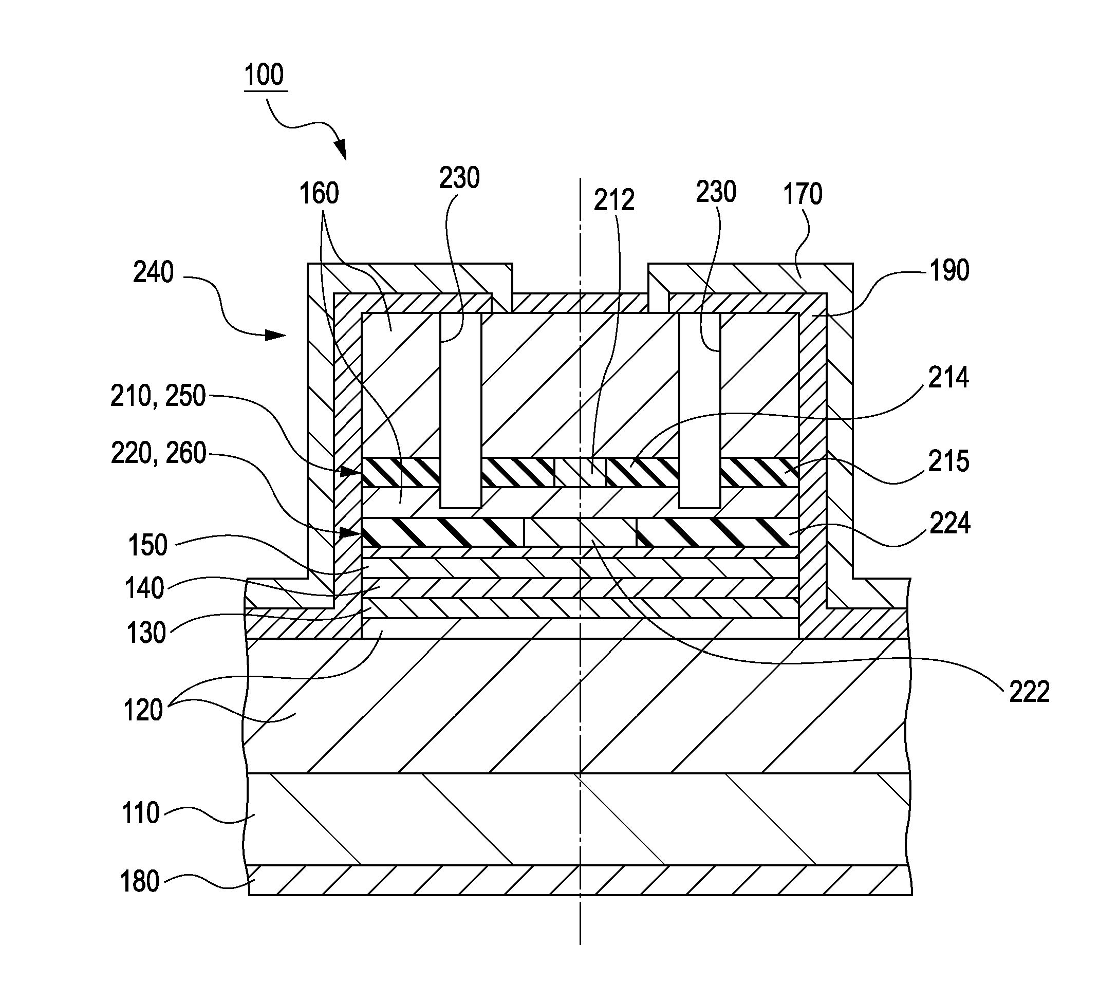
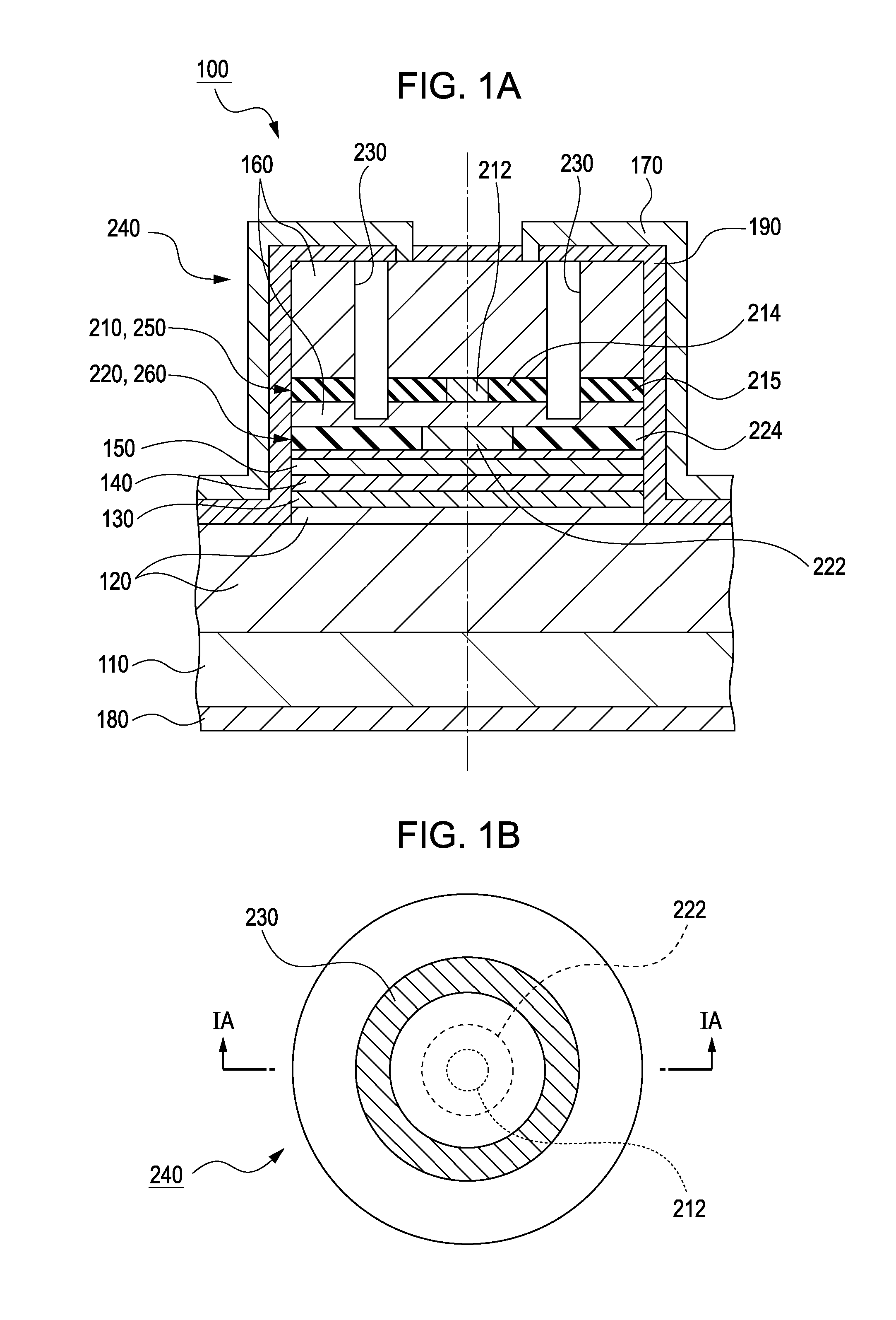
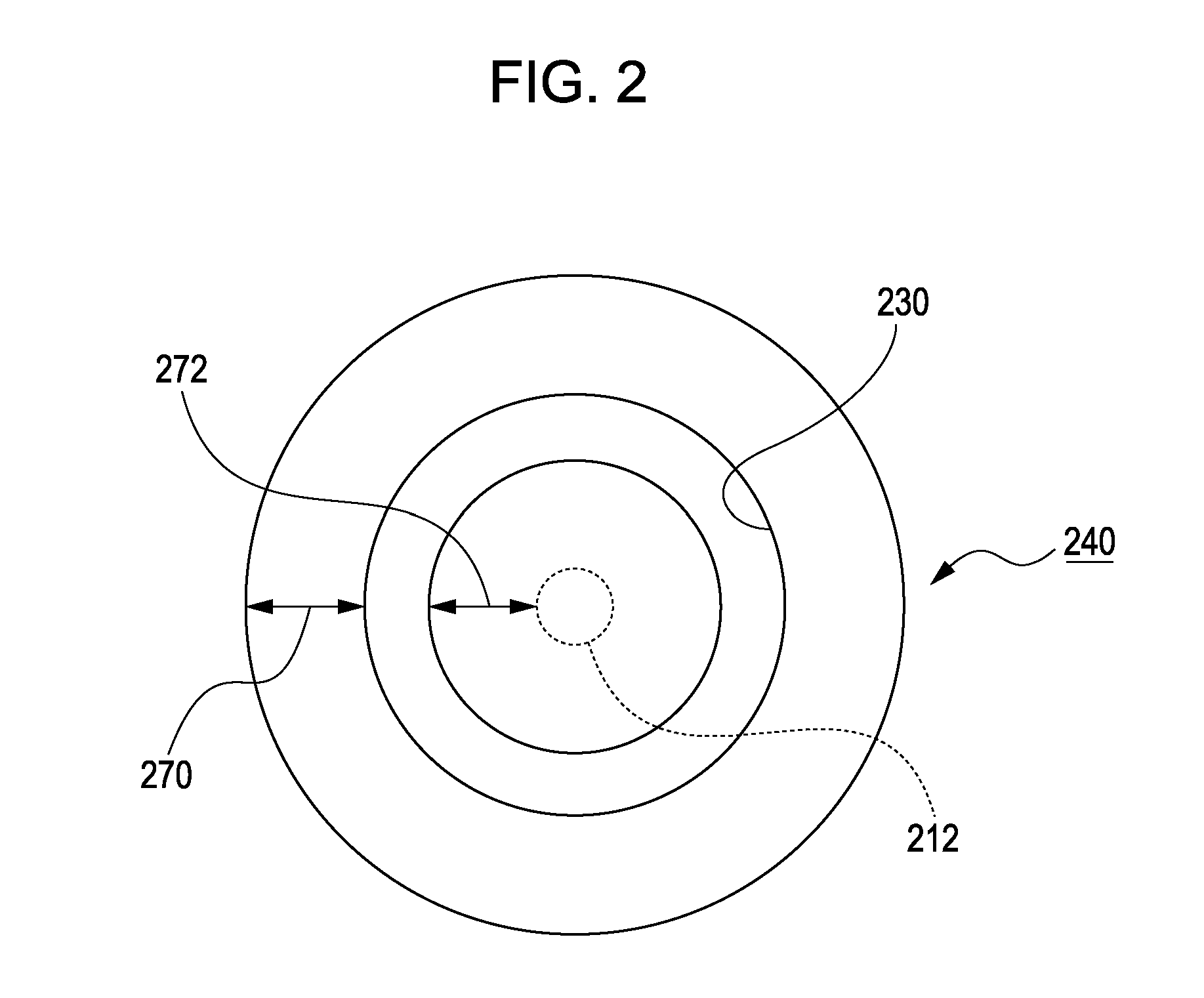
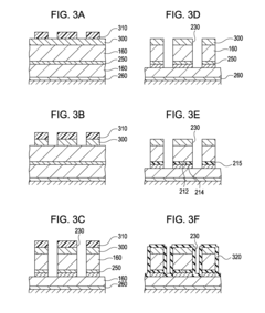
Vertical cavity surface emitting laser (VCSEL) array package and manufacturing method
PatentActiveUS12107387B2
Innovation
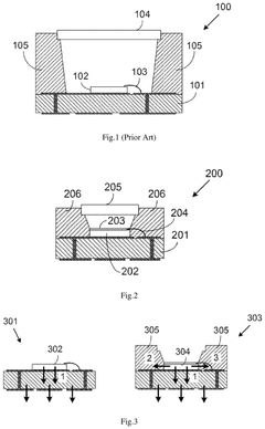
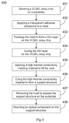
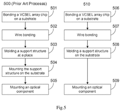
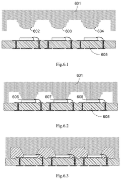
- A VCSEL array package design that includes a VCSEL array chip bonded on a substrate with a support structure molded from high thermal conductivity material, covering the side surfaces of the chip to create additional thermal paths and eliminate gaps, and a transparent thin layer to prevent beam obstruction and reflection.
Surface emitting laser with trenches to define conductive regions
PatentInactiveUS8188487B2
Innovation
- A surface emitting laser design with multiple current confinement structures, where a first trench structure forms a small aperture diameter with a shorter oxidation distance, and a second trench structure surrounds it, reducing oxidation distance variations and enhancing reliability.
Thermal Management Strategies for VCSEL Arrays
Thermal management represents a critical challenge in VCSEL array packaging for co-packaged optics applications. As power densities increase with higher integration levels, effective heat dissipation becomes essential for maintaining operational stability and extending device lifetime. VCSEL arrays are particularly sensitive to temperature variations, with performance parameters such as threshold current, slope efficiency, and wavelength stability all exhibiting strong temperature dependence.
Current thermal management approaches for VCSEL arrays can be categorized into passive and active cooling strategies. Passive techniques include optimized heat spreaders, typically utilizing materials with high thermal conductivity such as copper, diamond, or advanced ceramic composites. These materials facilitate efficient heat transfer from the active region to the package substrate. Thermal interface materials (TIMs) play a crucial role in minimizing contact resistance between different package components, with recent developments focusing on metal-based TIMs and phase-change materials that offer superior thermal performance.
Active cooling solutions incorporate thermoelectric coolers (TECs) or micro-channel liquid cooling systems directly integrated into the package. While these approaches provide more precise temperature control, they introduce additional complexity, power consumption, and reliability considerations. The industry trend is moving toward hybrid solutions that combine optimized passive cooling with selective active cooling elements for critical thermal hotspots.
Advanced thermal simulation techniques have become indispensable in the design process, enabling accurate prediction of temperature distributions and identification of potential thermal bottlenecks. Computational fluid dynamics (CFD) models coupled with detailed electro-thermal simulations allow designers to evaluate various cooling strategies before physical prototyping, significantly reducing development cycles and costs.
Emerging thermal management innovations include three-dimensional heat spreading architectures that utilize vertical thermal vias and embedded cooling channels. These structures maximize the effective heat dissipation area while maintaining compact package dimensions. Additionally, graphene-based thermal interface materials show promising results in laboratory settings, potentially offering thermal conductivity values exceeding 2000 W/mK when properly integrated.
For co-packaged optics applications specifically, thermal crosstalk between VCSEL arrays and adjacent silicon photonics or electronic components presents unique challenges. Thermal isolation structures and strategic component placement have proven effective in minimizing unwanted thermal interactions. The development of thermally-aware design methodologies that consider the entire optical-electronic system rather than individual components in isolation represents a significant advancement in addressing these complex thermal management requirements.
Supply Chain Considerations for VCSEL Manufacturing
The VCSEL manufacturing supply chain represents a complex ecosystem that significantly impacts the feasibility and cost-effectiveness of VCSEL array packaging for co-packaged optics applications. This ecosystem encompasses raw material suppliers, epitaxial wafer manufacturers, device fabrication facilities, testing equipment providers, and packaging specialists.
Material sourcing constitutes a critical consideration in the VCSEL supply chain. High-purity gallium arsenide (GaAs) substrates and epitaxial materials require specialized suppliers with advanced quality control capabilities. The limited number of qualified suppliers for these materials creates potential bottlenecks, especially during periods of high demand. Additionally, the geographical concentration of certain raw material sources, particularly rare earth elements used in some VCSEL designs, introduces geopolitical risk factors that must be considered in long-term supply planning.
Manufacturing capacity represents another significant supply chain consideration. The production of VCSEL arrays requires specialized fabrication facilities with class 100 or better cleanroom environments. Currently, these facilities are concentrated among a handful of manufacturers in North America, Europe, and Asia. This concentration creates potential vulnerabilities in the supply chain, particularly when rapid scaling is required to meet market demands for co-packaged optics applications.
Quality control and testing infrastructure constitute essential components of the VCSEL supply chain. The performance parameters of VCSELs for co-packaged optics applications require sophisticated testing equipment and methodologies. The availability of these testing capabilities can become a limiting factor in production scaling, particularly for high-volume applications.
Packaging and integration capabilities represent perhaps the most critical aspect of the VCSEL supply chain for co-packaged optics. The specialized nature of optical alignment and packaging for these applications requires advanced equipment and expertise. Currently, this segment of the supply chain exhibits significant fragmentation, with various specialized providers focusing on different aspects of the packaging process.
Supply chain resilience has emerged as a strategic consideration following recent global disruptions. Manufacturers are increasingly implementing multi-sourcing strategies for critical components and materials. Additionally, there is a growing trend toward vertical integration among larger manufacturers to secure critical supply chain elements and reduce dependencies on external suppliers.
Cost structures within the VCSEL supply chain significantly impact the economic viability of co-packaged optics solutions. Material costs typically represent 30-40% of total production expenses, while specialized packaging processes can account for up to 50% of the final component cost. These cost structures highlight the importance of supply chain optimization in achieving commercially viable solutions for mass-market applications.
Unlock deeper insights with PatSnap Eureka Quick Research — get a full tech report to explore trends and direct your research. Try now!
Generate Your Research Report Instantly with AI Agent
Supercharge your innovation with PatSnap Eureka AI Agent Platform!