

Plane Faraday screening system of radio frequency inductive coupled plasma source
A Faraday shielding and plasma source technology, applied in the direction of plasma and electrical components, can solve problems such as instantaneous impedance mismatch, difficulty in discharge breakdown, discharge instability, etc., and achieve small antenna current standing wave effect and sputtering Small pollution and good angular uniformity
- Summary
- Abstract
- Description
- Claims
- Application Information
AI Technical Summary
Problems solved by technology
Method used
Image


Examples
Embodiment Construction
[0032] The specific implementation manners of the present invention will be described in detail below in combination with technical solutions and accompanying drawings.
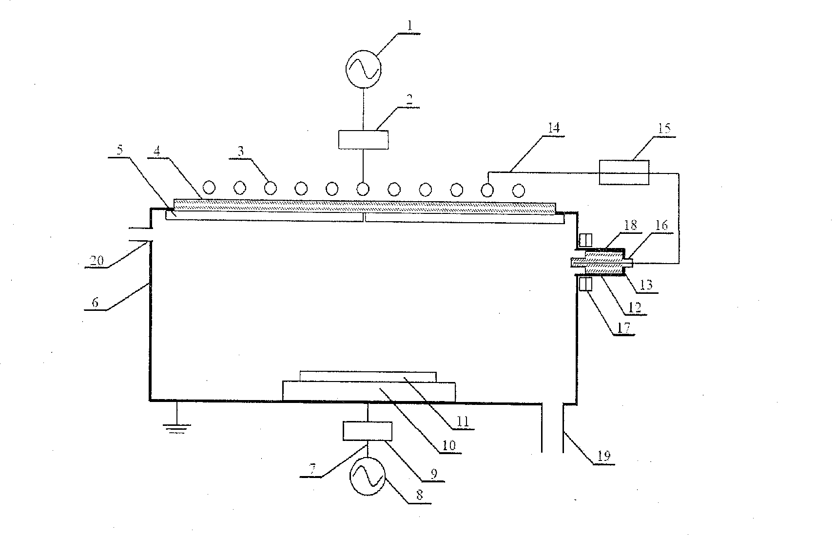
[0033] Such as figure 1 As shown, the energy generated by the RF power supply 1 reaches the RF coupling antenna 3 through the impedance matching device 2, and the variable capacitor C is adjusted 1 、C 2 ( Figure 2a ) and C 3 Minimize the reflected power. Faraday shield 5 to ground ( image 3 ), the capacitive coupling current driven by the RF antenna voltage reaches the ground through the Faraday shield 5, and the capacitive coupling inside the plasma is blocked. The Faraday shield adopts a crack structure, and the radio frequency antenna current can pass through the crack to generate an alternating magnetic field in the vacuum chamber, and the vortex electric field generated by the changing magnetic field accelerates the discharge of electron ionized neutral particles.
[0034] Faraday shielding struc...
PUM
 Abstract
Description
Claims
Application Information