Vertical dual-sided CCD line scanning automatic detection platform for PCB (Printed Circuit Board)

A PCB circuit board and automatic detection technology, which is applied in the direction of optical testing defects/defects, can solve the problems of cumbersome mechanism, low inspection efficiency, high mechanism cost, etc., and achieve the effect of improving use stability, long service life, and improving production efficiency

Inactive Publication Date: 2012-12-26
JOINT STARS TECH
View PDF7 Cites 14 Cited by
  • Summary
  • Abstract
  • Description
  • Claims
  • Application Information

AI Technical Summary

Problems solved by technology

[0002] At present, in the field of visual inspection, when multi-sided inspection is required for product appearance inspection, the usual method is to scan one side of the object, then turn the object over and scan the other side to complete the multi-sided scanning inspection of the object. This method needs to complete the work of flipping the object once in the middle, the mechanism is cumbersome, the inspection efficiency is low, and the mechanism cost is high

Method used


Image

  • Vertical dual-sided CCD line scanning automatic detection platform for PCB (Printed Circuit Board)
  • Vertical dual-sided CCD line scanning automatic detection platform for PCB (Printed Circuit Board)
  • Vertical dual-sided CCD line scanning automatic detection platform for PCB (Printed Circuit Board)

Examples


Embodiment Construction

[0041] Below the present invention will be further described in conjunction with the embodiment in the accompanying drawings:

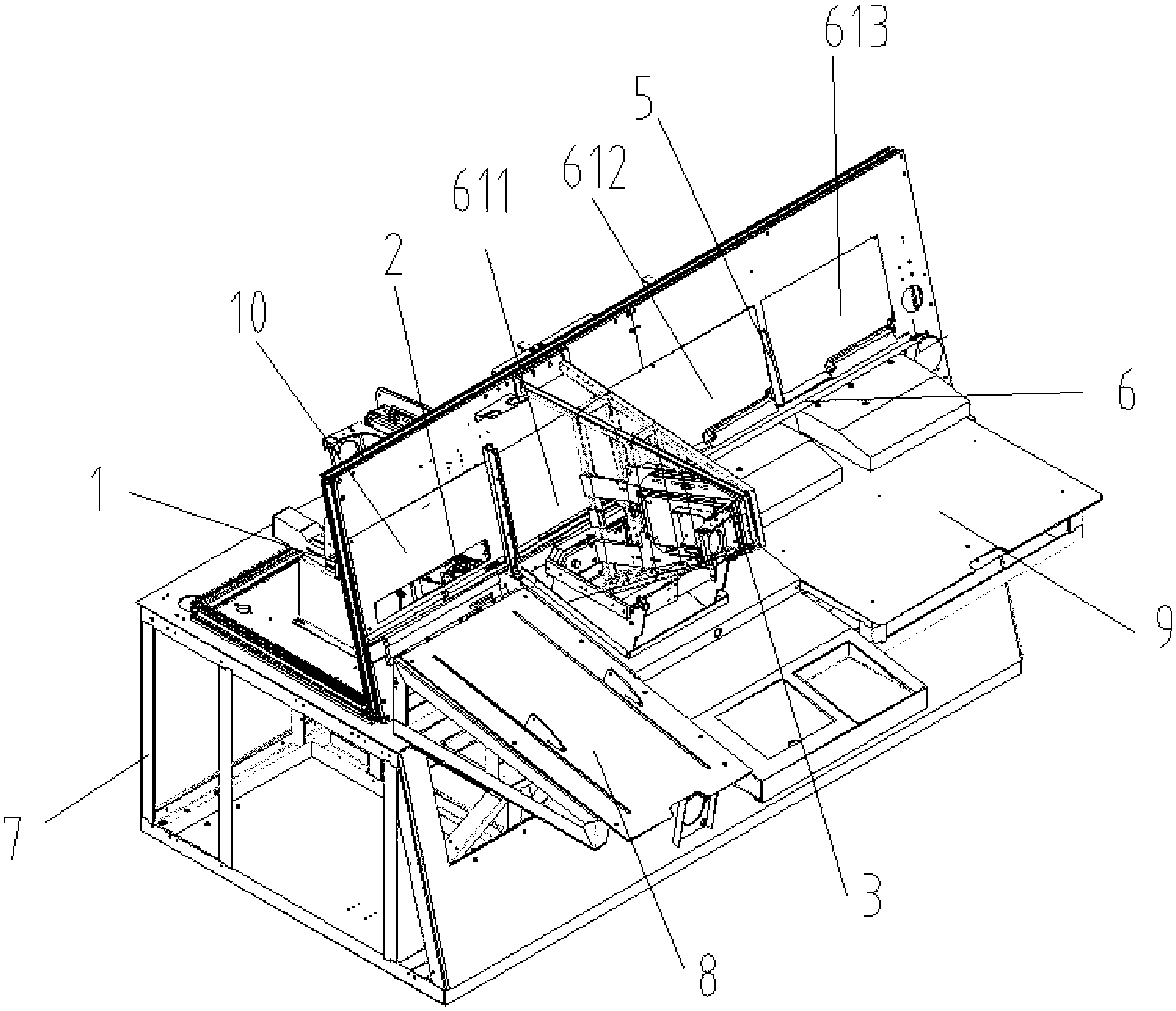
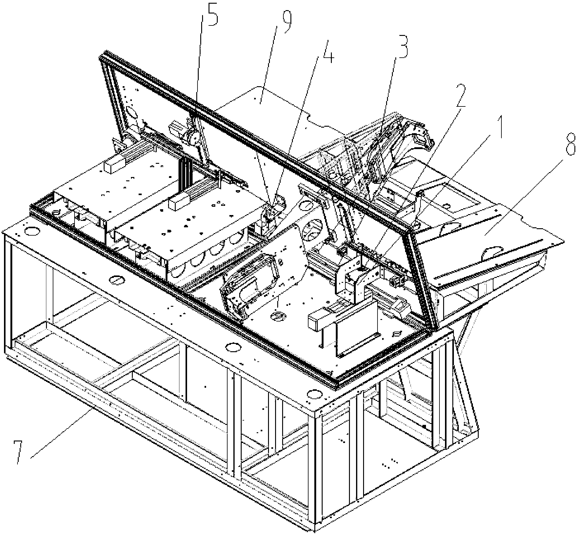
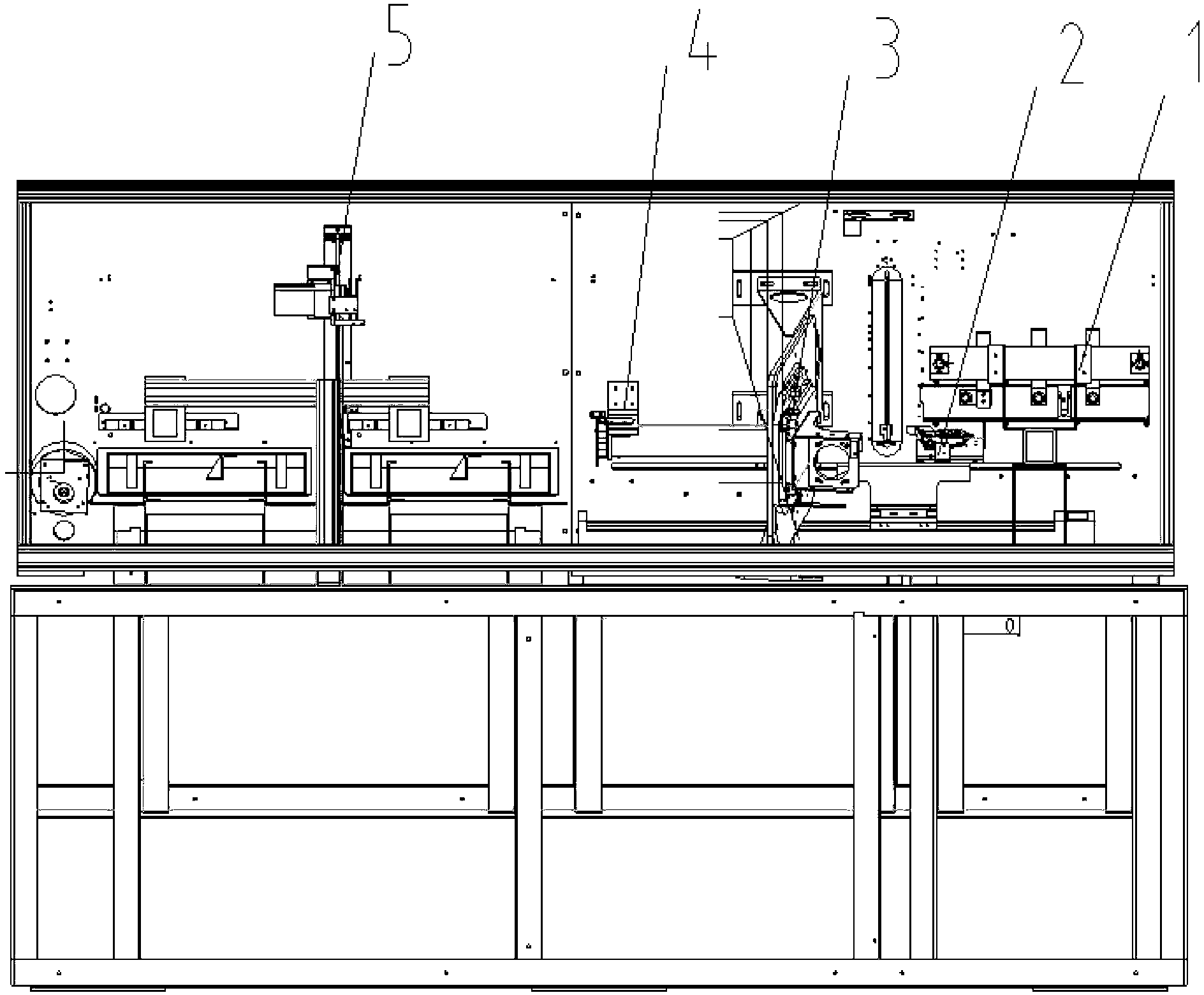
[0042] like Figures 1 to 3 , a PCB circuit board vertical double-sided CCD line scanning automatic detection platform, including a fast cylinder type suction nozzle adjustment mechanism 1, a cam arc dial positioning mechanism 2, a vertical double-sided CCD line scanning mechanism 3 in the detection area, and a cam arc Line push plate mechanism 4, cam baffle plate mechanism 5, steel belt conveying device 6, frame 7, inspection platform 8, post-inspection plate platform 9, sub-board inspection area 10, double-sided vertical line scanning area 611, defective The board rejecting area 612 and the qualified board collecting area 613, the board sub-board inspection area 10, the double-sided vertical line scanning area 611, the defective board rejecting area 612 and the qualified board collecting area 613 are arranged in a straight line on the rack 7 in sequ...


PUM


Abstract

The invention relates to a vertical dual-sided CCD line scanning automatic detection platform for a PCB (Printed Circuit Board). The comprises vertical dual-sided CCD line scanning automatic detection platform comprises a rapid cylinder type nozzle regulation mechanism (1), a cam arc dialing board positioning mechanism (2), a detection area vertical dual-sided CCD line scanning mechanism (3), a cam arc push plate mechanism (4), a cam baffle mechanism (5), a steel belt transport device (6), a rack (7), an inspection platform (8), an inspection post-position plate platform (9), a board distributing inspection region (10), a dual-sided vertical line scanning region (611), a bad board rejecting region (612) and a qualified board collecting region (613). According to the vertical dual-sided CCD line scanning automatic detection platform, due to the adoption of two-sided simultaneous scanning, the PCB is not needed to be overturned, thus the complexity of a mechanical structure is reduced; and because an overturning action is not needed, the efficiency reduction caused by overturning is eliminated. One time of production benefit can be increased, the volume of the vertical dual-sided CCD line scanning automatic detection platform is greatly reduced, and more vertical dual-sided CCD line scanning automatic detection platforms can be placed in same space, thus the utilization rate of a factory is effectively increased.

Description

technical field [0001] The invention relates to the technical field of mechanical and electronic visual inspection, in particular to a PCB circuit board vertical double-sided CCD line scanning automatic detection platform. Background technique [0002] At present, in the field of visual inspection, when multi-sided inspection is required for product appearance inspection, the usual method is to scan one side of the object, then flip the object and scan the other side to complete the multi-sided scanning inspection of the object. This method needs to complete the work of turning over the object once in the middle, the mechanism is cumbersome, the inspection efficiency is low, and the mechanism cost is high. Contents of the invention [0003] In order to simplify the current cumbersome mechanism for multi-faceted visual inspection of items, save costs, and improve the efficiency of product production inspection, a PCB circuit board vertical double-sided CCD line scanning aut...

Claims


Application Information

Patent Timeline
Patent Type & Authority Applications(China)
IPC IPC(8): G01N21/88
Inventor 覃早才
Owner JOINT STARS TECH
Why Eureka
Try Eureka