Chip and electronic device

An electronic device and chip technology, applied in the electronic field, can solve problems such as damage, poor quality of electronic devices, unstable chip operation, etc., and achieve the effects of protection stability, avoiding external electrostatic protection circuits, and functional integration

Inactive Publication Date: 2015-11-25
TCL CHINA STAR OPTOELECTRONICS TECH CO LTD
View PDF4 Cites 4 Cited by
  • Summary
  • Abstract
  • Description
  • Claims
  • Application Information

AI Technical Summary

Problems solved by technology

Frictional electrification and human body static electricity are two major hazards in the electronics industry, which often cause the chip in the electronic device to run unstable or even damaged, resulting in poor quality of the electronic device

Method used


Image

  • Chip and electronic device
  • Chip and electronic device
  • Chip and electronic device

Examples


Embodiment Construction

[0018] The following will clearly and completely describe the technical solutions in the embodiments of the present invention with reference to the accompanying drawings in the embodiments of the present invention. Obviously, the described embodiments are only some, not all, embodiments of the present invention. Based on the embodiments of the present invention, all other embodiments obtained by persons of ordinary skill in the art without making creative efforts belong to the protection scope of the present invention.

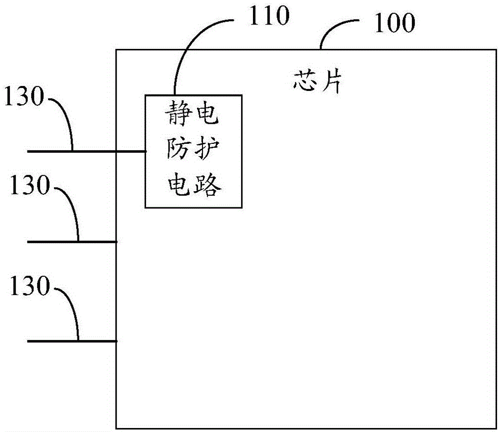
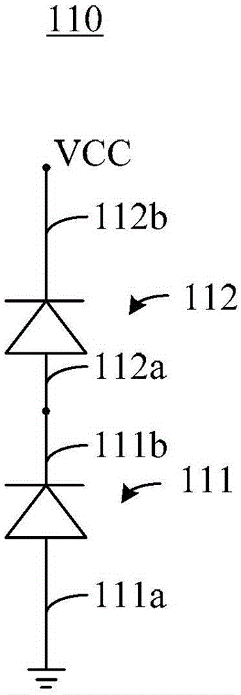
[0019] Please also refer to figure 1 and figure 2 , figure 1 It is a schematic diagram of the circuit structure of a chip in a preferred embodiment of the present invention. figure 2 It is a circuit diagram of the electrostatic protection circuit in the chip in a preferred embodiment of the present invention. The chip 100 may be disposed in an electronic device. The electronic devices include, but are not limited to, portable devices such as smart phones...


PUM


Abstract

The invention provides a chip and an electronic device. The chip comprises at least one pin and is characterized in that the internal part of the chip is provided with at least one electrostatic protection circuit, the electrostatic protection circuit is used for reducing or eliminating damages imposed on other components or circuits inside the chip by static electricity, the electrostatic protection circuit is set corresponding to one of the pins, and the electrostatic protection circuit is electrically connected with the pin. The electronic device comprises the chip provided by the invention.

Description

technical field [0001] The invention relates to the field of electronics, in particular to a chip and an electronic device. Background technique [0002] Static electricity is an objectively existing natural phenomenon, which can be produced in many ways, such as contact, friction, induction between electrical appliances, etc. Static electricity is characterized by long-term accumulation, high voltage, low power, small current and short action time. The action of the human body or the contact, separation, friction or induction with other objects can generate thousands of volts or even tens of thousands of volts of static electricity. Frictional electrification and human body static electricity are two major hazards in the electronics industry, which often cause the chip in the electronic device to run unstable or even be damaged, resulting in poor quality of the electronic device. Contents of the invention [0003] The present invention provides a chip, the chip includes...

Claims


Application Information

Patent Timeline
Patent Type & Authority Applications(China)
IPC IPC(8): H02H9/04
CPCH02H9/046H01L27/0255
Inventor 张先明陈宥烨陈明暐曹丹
Owner TCL CHINA STAR OPTOELECTRONICS TECH CO LTD
Why Eureka
Try Eureka