Array substrate, touch display panel and touch display device

A technology for array substrates and display areas, which is applied in the fields of instruments, computing, and electrical digital data processing, etc., can solve the problems of increasing process complexity and increasing the thickness of the display screen, and achieve the effect of reducing the resistance of touch electrodes and simplifying the process

Active Publication Date: 2016-04-06
SHANGHAI AVIC OPTOELECTRONICS +1
View PDF3 Cites 58 Cited by
  • Summary
  • Abstract
  • Description
  • Claims
  • Application Information

AI Technical Summary

Problems solved by technology

In order to avoid forming an electric field between the third metal layer and other conductive layers (such as the second metal layer and the common electrode), it is also necessary to mak

Method used


Image

  • Array substrate, touch display panel and touch display device
  • Array substrate, touch display panel and touch display device
  • Array substrate, touch display panel and touch display device

Examples


Embodiment Construction

[0023] The application will be further described in detail below in conjunction with the accompanying drawings and embodiments. It should be understood that the specific embodiments described here are only used to explain related inventions, rather than to limit the invention. It should also be noted that, for the convenience of description, only the parts related to the related invention are shown in the drawings.

[0024] It should be noted that, in the case of no conflict, the embodiments in the present application and the features in the embodiments can be combined with each other. The present application will be described in detail below with reference to the accompanying drawings and embodiments.

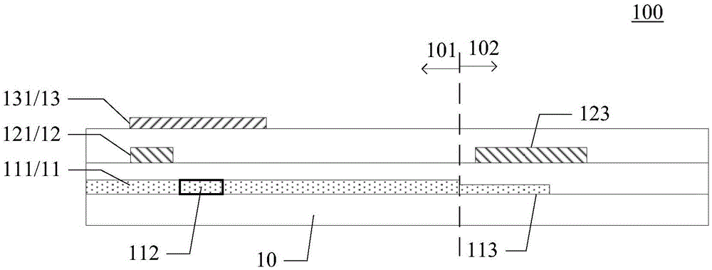
[0025] Please refer to figure 1 , which shows a partial cross-sectional view of the array substrate provided by the present application. Such as figure 1 As shown, the array substrate 100 includes a base substrate 10 , and the base substrate 10 includes a display area 101 ...


PUM


Abstract

The invention discloses an array substrate, a touch display panel and a touch display device. According to one embodiment, the array substrate comprises a substrate body, a plurality of metal layers, a touch control electrode layer and a plurality of touch control signal lines, wherein the substrate body has a display area and a non-display area, the metal layers are perpendicular to the substrate body and include the first metal layers and the second metal layers, the first metal layers are used for forming scanning lines of the array substrate, and the second metal layers are used for forming data lines of the array substrate; a plurality of pixel units are arranged in the display area and distributed into an array, the line direction of the pixel units is the extending direction of the scanning lines, and the row direction of the pixel units is the extending direction of the data lines; the touch control electrode layer comprises a plurality of touch control electrodes, the touch control signal lines are electrically connected with one touch control electrode and used for transmitting touch control signals to the touch control electrode, and the touch control signal lines and at least one metal layer are located on the same layer. In this way, the complexity of the manufacturing process of the array substrate can be reduced.

Description

technical field [0001] The present application relates to the field of display technology, in particular to the field of touch display technology, especially to an array substrate, a touch display panel and a touch display device. Background technique [0002] Common electrodes are arranged on the embedded touch display screen. During touch detection, the common electrode is multiplexed as a touch emission electrode to receive a touch driving signal, and the touch detection circuit determines a touch point according to a change in capacitance on the display screen. The common electrode can be made of ITO conductive glass. In the in-cell touch display panel, the common electrodes on the touch display panel are arranged in strips in parallel. Since the area of ​​the common electrode is relatively large, its resistance value is relatively high, which greatly affects the accuracy of the touch detection circuit. [0003] Generally, an in-cell touch display screen may include m...

Claims


Application Information

Patent Timeline
IPC IPC(8): G06F3/041G06F3/044
CPCG06F3/0412G06F3/044
Inventor 简守甫曹兆铿夏志强
Owner SHANGHAI AVIC OPTOELECTRONICS
Why Eureka
Try Eureka