Display panel and pixel circuit

A pixel circuit and display panel technology, applied in the field of pixel circuits, can solve problems such as too late to update pixels, complex circuit design, and increased energy consumption of display devices, and achieve the effect of avoiding flickering

Inactive Publication Date: 2017-03-01
GIO OPTOELECTRONICS CORP
View PDF0 Cites 33 Cited by
  • Summary
  • Abstract
  • Description
  • Claims
  • Application Information

AI Technical Summary

Problems solved by technology

However, in the above example, it is necessary to increase the scanning frequency of the scanning signal by 4 times
This is obviously impractical, because such an approach will not only increase the power consumption of the display device, but also make the circuit design more complicated
In addition, since the load on each scanning line will vary, when the scanning frequency of the scanning signal increases, the pixels behind each scanning line may not be refreshed in time. also have the above phenomenon

Method used


Image

  • Display panel and pixel circuit
  • Display panel and pixel circuit
  • Display panel and pixel circuit

Examples


Embodiment Construction

[0036] A pixel circuit and a display panel according to preferred embodiments of the present invention will be described below with reference to related drawings, wherein the same elements will be described with the same reference numerals.

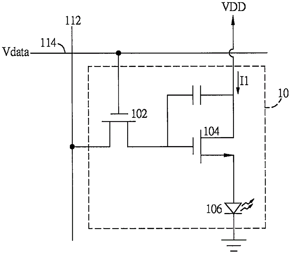
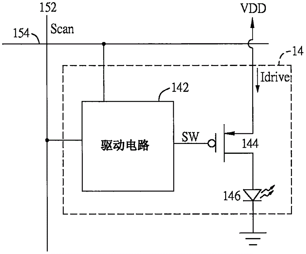
[0037] figure 2 A block diagram of a pixel circuit according to a preferred embodiment of the present invention is shown. Please refer to figure 2 The pixel circuit 2 provided in this embodiment includes a light emitting element 22, a switch unit 24, a driving signal generating unit 26 and a working power supply VDD. One end of the switch unit 24 is electrically connected to the light emitting element 22 , and the other end is electrically connected to the working power VDD. In addition, the switch unit 24 is also electrically connected to the driving signal generating unit 26 . The pixel circuit of the present invention is an active matrix array circuit, which can be applied to various display devices, such as outdoor advertising bi...


PUM


Abstract

A pixel circuit includes a lighting element, a driving signal generating unit and a switching unit. The driving signal generating unit compares a data signal with a reference signal so as to generate a PWM driving signal. The status of the PWM driving signal is determined according to the comparing result of the data signal and the reference signal. The switching unit is electrically connected to a power source and the lighting element, and generates a driving current to drive the lighting element to emit light according to the PWM driving signal.

Description

technical field [0001] The invention relates to a pixel circuit, in particular to a pixel circuit of a light emitting diode display panel. Background technique [0002] Figure 1A Shown is an equivalent circuit diagram of a well-known analog-driven OLED pixel. Please refer to Figure 1A , the well-known organic light emitting diode (hereinafter referred to as OLED) pixel 10 can be applied in a display device, and the OLED pixel 10 includes a transistor 102 and a transistor 104 . Wherein, the source terminal of the transistor 102 is electrically connected to the data line 112 , and the gate terminal is electrically connected to the scan line 114 . In addition, the drain terminal of the transistor 102 is electrically connected to the gate terminal of the transistor 104 , and the drain terminal and the source terminal of the transistor 104 are electrically connected to the operating power VDD and the organic light emitting diode 106 respectively. [0003] When the scan line 1...

Claims


Application Information

Patent Timeline
Patent Type & Authority Applications(China)
IPC IPC(8): G09G3/3208G09G3/3241G09G3/32
CPCG09G3/32G09G3/3208G09G3/3241G09G3/3258G09G2300/0833G09G2300/0842G09G2300/0861G09G2310/0259G09G2310/066G09G2320/0247G09G3/3233G09G2310/06
Inventor 杨武璋杨嘉和
Owner GIO OPTOELECTRONICS CORP
Why Eureka
Try Eureka