Array substrate, irregularly-shaped display and display device

A technology of array substrate and display area, applied in static indicators, instruments, semiconductor devices, etc., can solve the problems of affecting display, inconsistent pixel voltage coupling voltage drop, and unequal number of pixels, etc.

Active Publication Date: 2017-09-29
SHANGHAI TIANMA MICRO ELECTRONICS CO LTD
View PDF4 Cites 65 Cited by
  • Summary
  • Abstract
  • Description
  • Claims
  • Application Information

AI Technical Summary

Problems solved by technology

[0004] However, in the special-shaped display, due to the inconsistency of the length of the grid lines in the display area, the number of pixels connected to the grid lines of different lengths is not equal, so that the capacitance

Method used


Image

  • Array substrate, irregularly-shaped display and display device
  • Array substrate, irregularly-shaped display and display device
  • Array substrate, irregularly-shaped display and display device

Examples


Embodiment Construction

[0031] In order to make the purpose, technical solutions and advantages of the present invention clearer, the present invention will be further described in detail below in conjunction with the accompanying drawings. Obviously, the described embodiments are only some of the embodiments of the present invention, rather than all of them. Based on the embodiments of the present invention, all other embodiments obtained by persons of ordinary skill in the art without making creative efforts belong to the protection scope of the present invention.

[0032] The shapes and sizes of the components in the drawings do not reflect the real scale, but are only intended to schematically illustrate the content of the present invention.

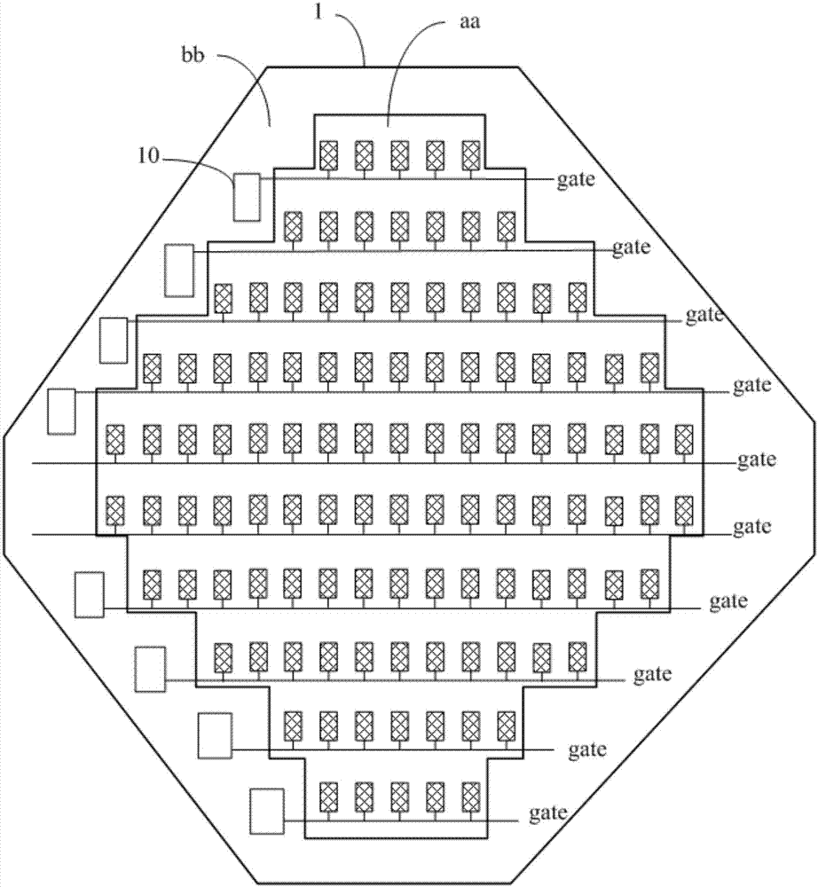
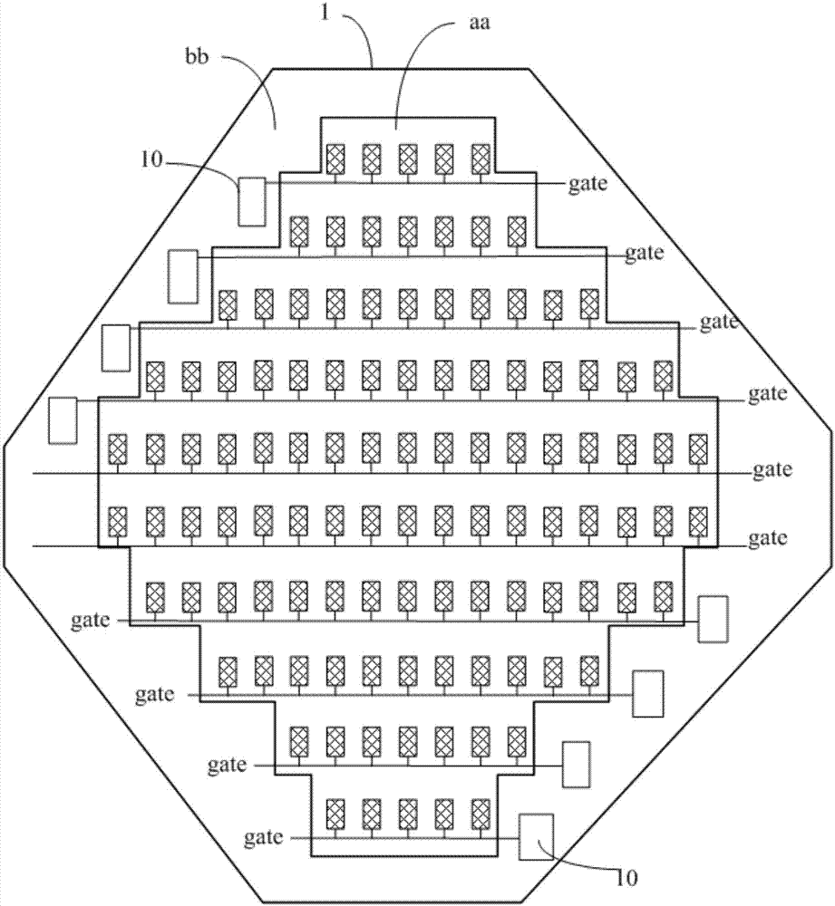
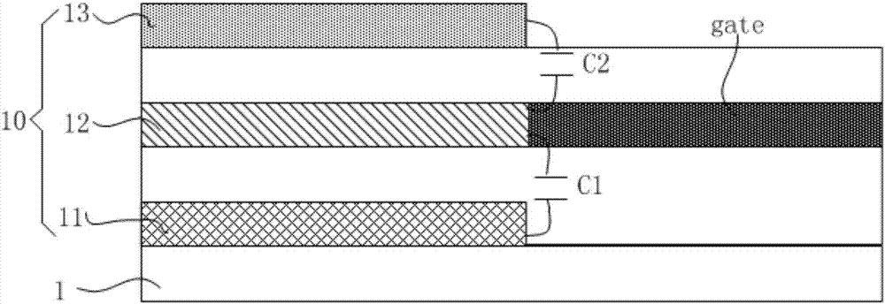
[0033] An array substrate provided by an embodiment of the present invention, such as Figure 1a and Figure 1b As shown, among them, Figure 1a A schematic structural diagram of an array substrate provided by an embodiment of the present invention; Figur...


PUM


Abstract

The invention discloses an array substrate, an irregularly-shaped display and a display device, and relates to the technical field of display. In the array substrate, a plurality of grid lines with unequal lengths are arranged on a display region, capacitance compensation structures are arranged on a non-display region and are in one-to-one corresponding to a part of the grid lines, each capacitance compensation structure comprises a first electrode, a second electrode and a third electrode which are arranged on a substrate, the first electrode and the second electrode form a first capacitor, the second electrode and the third electrode form a second capacitor, and a coupling capacitance value of the capacitance compensation structure is relevant to the length of the corresponding grid line. According to the technical scheme provided by the invention, the capacitance compensation structures are arranged on the non-display region of the array substrate, the coupling capacitance values of the capacitance compensation structures are relevant to the lengths of the corresponding grid lines, thus, the difference among coupling capacitance of the grid lines with different lengths on the display region is compensated, and the display image quality is improved.

Description

technical field [0001] The present invention relates to the field of display technology, and more specifically, to an array substrate, a special-shaped display and a display device. Background technique [0002] With the rapid development of display technology, in addition to the traditional information display and other functions of the display, in order to better adapt to the overall structure and use requirements of the environment, the requirements for appearance are gradually increasing, and special-shaped displays have emerged. [0003] The special-shaped display is a special-shaped display transformed on the basis of the traditional display, so that the characteristics of the display can better adapt to the overall structure and environment of the building. At present, the common special-shaped screens mainly have fan-shaped, arc-shaped, circular, cylindrical, triangular and other structural forms. [0004] However, in the special-shaped display, due to the inconsist...

Claims


Application Information

Patent Timeline
IPC IPC(8): H01L27/12
CPCH01L27/124H01L27/1255G09G3/20G09G2300/0426G09G2300/043G09G2320/0223G09G2320/0233
Inventor 席克瑞周一安许文钦
Owner SHANGHAI TIANMA MICRO ELECTRONICS CO LTD
Why Eureka
Try Eureka