Chip testing device for display and display with same

A chip testing and display technology, applied in static indicators, instruments, etc., can solve problems such as inability to measure signals, affecting product analysis and testing, and achieve the effect of improving accuracy and effectiveness, and improving the efficiency of bad analysis.

Inactive Publication Date: 2020-08-28
BOE TECH GRP CO LTD +1
View PDF4 Cites 0 Cited by
  • Summary
  • Abstract
  • Description
  • Claims
  • Application Information

AI Technical Summary

Problems solved by technology

However, in the related art, there is an insulating layer on the surface of the signal line and there are no test points, so that the required signal cannot be measured, which greatly affects the analytical test of the product

Method used


Image

  • Chip testing device for display and display with same
  • Chip testing device for display and display with same
  • Chip testing device for display and display with same

Examples


Embodiment Construction

[0024] Embodiments of the present invention are described in detail below, examples of which are shown in the drawings, wherein the same or similar reference numerals designate the same or similar elements or elements having the same or similar functions throughout. The embodiments described below by referring to the figures are exemplary and are intended to explain the present invention and should not be construed as limiting the present invention.

[0025] Refer to the attached Figure 1-6 A chip testing device for a display according to an embodiment of the present invention and a display having the same will be described.

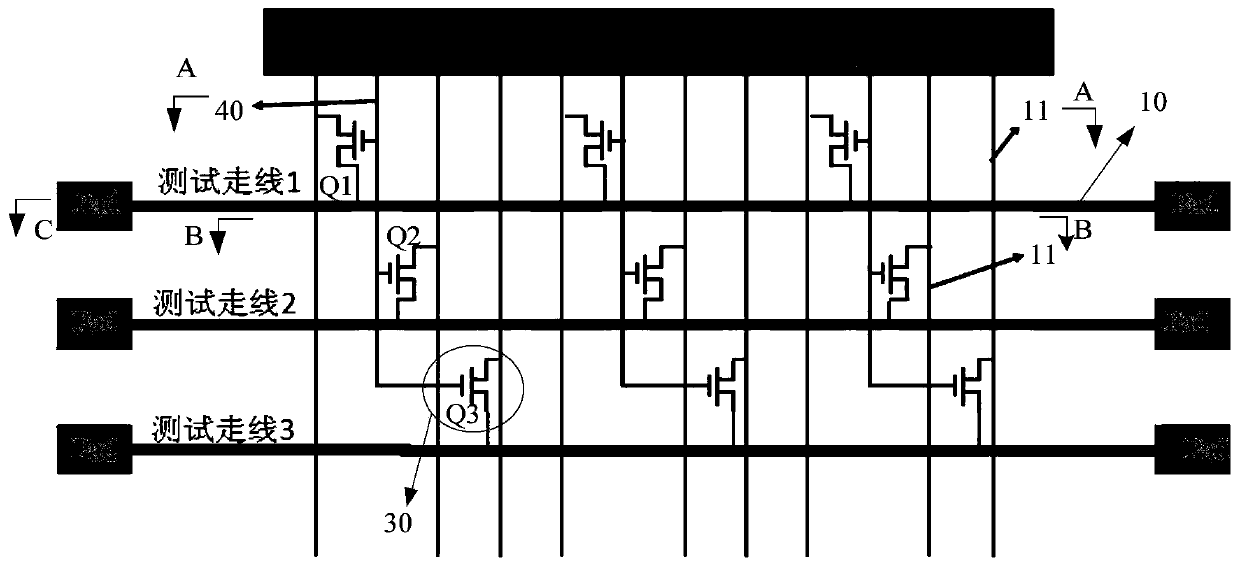
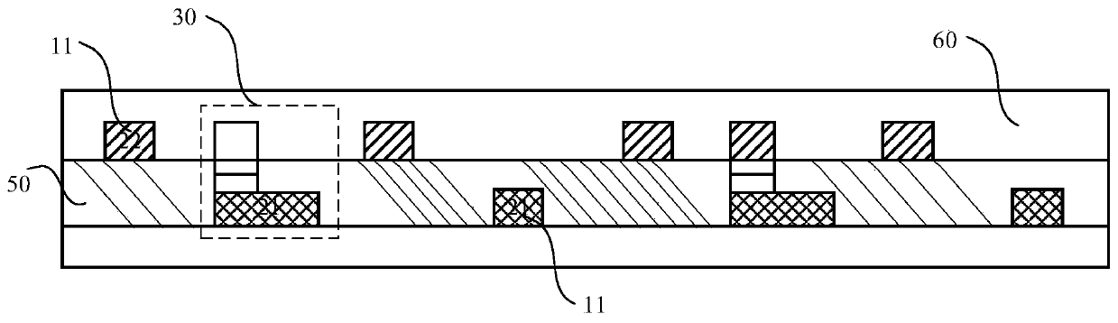
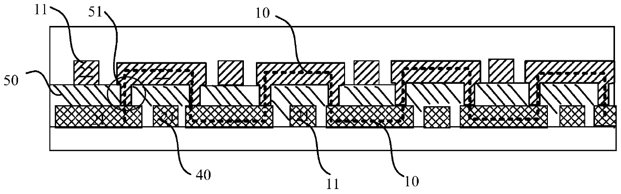
[0026] according to Figure 1-3 In an embodiment of the present invention, the device for testing a chip of a display according to the embodiment of the present invention includes: M test wires 10, N switch units 30 and a control unit.

[0027] Wherein, each test line 10 is interspersed with N signal lines 11 to be tested on the chip, wherein, when th...


PUM


Abstract

The invention discloses a chip testing device of a display and a display with the chip testing device. The device comprises M testing wires, N switch units and a control unit, the testing wires are arranged on N to-be-tested signal lines on a chip in a penetrating manner; when the testing wires face the to-be-tested signal lines of a first film of the chip, the testing wires are arranged on a second film of the chip; when the testing wires face the to-be-tested signal lines on the second film, the testing wires are arranged on the first film; the testing wires are used for receiving signals on at least one to-be-tested signal line; first ends of the N switch units are separately connected with the N to-be-tested signal lines correspondingly; a second end of each switch unit is connected with an optional one of the M testing wires; each switch unit is used for controlling the corresponding to-be-tested signal line to communicate with the corresponding testing wire; and the control unit is used for controlling the N switch units, so that required signals can be measured rapidly and effectively, and accuracy and effectiveness of signal measurement are improved.

Description

technical field [0001] The invention relates to the field of display technology, in particular to a display chip testing device and a display with the device. Background technique [0002] Displays such as TFT LCD often have poor wiring and other defects during reliability testing and normal use. In the related art, it is usually necessary to measure the output signal of the driver chip or other wires when performing fault analysis. However, in the related art, there is an insulating layer on the surface of the signal line and there is no test point, so that the required signal cannot be measured, which greatly affects the analytical test of the product. Contents of the invention [0003] The present invention aims to solve one of the technical problems in the related art at least to a certain extent. Therefore, an object of the present invention is to provide a chip testing device for a display, which can quickly and effectively measure a required signal without distort...

Claims


Application Information

Patent Timeline
Patent Type & Authority Patents(China)
IPC IPC(8): G09G3/00
CPCG09G3/006
Inventor 黄炯汪祥李朋
Owner BOE TECH GRP CO LTD
Why Eureka
Try Eureka