Electronic device and antenna processing method

A technology for electronic equipment and antennas, applied to antennas, loop antennas, antenna supports/installation devices, etc., can solve problems such as antenna signal interference, and achieve the effect of reducing signal interference and saving space.

Active Publication Date: 2018-06-15
LENOVO (BEIJING) CO LTD
View PDF9 Cites 5 Cited by
  • Summary
  • Abstract
  • Description
  • Claims
  • Application Information

AI Technical Summary

Problems solved by technology

[0004] In view of this, the present invention provides an electronic device and an antenna processing method to solve the problem of signal interference between antennas caused by setting various antennas in a specific area of ​​an electronic device with limited space in the prior art. The specific solution is as follows:

Method used


Image

  • Electronic device and antenna processing method
  • Electronic device and antenna processing method
  • Electronic device and antenna processing method

Examples


Embodiment Construction

[0046] The following will clearly and completely describe the technical solutions in the embodiments of the present invention with reference to the accompanying drawings in the embodiments of the present invention. Obviously, the described embodiments are only some, not all, embodiments of the present invention. Based on the embodiments of the present invention, all other embodiments obtained by persons of ordinary skill in the art without making creative efforts belong to the protection scope of the present invention.

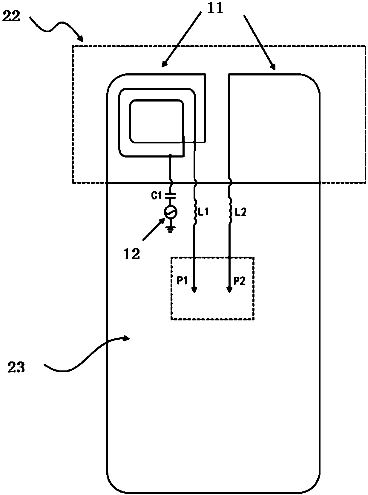
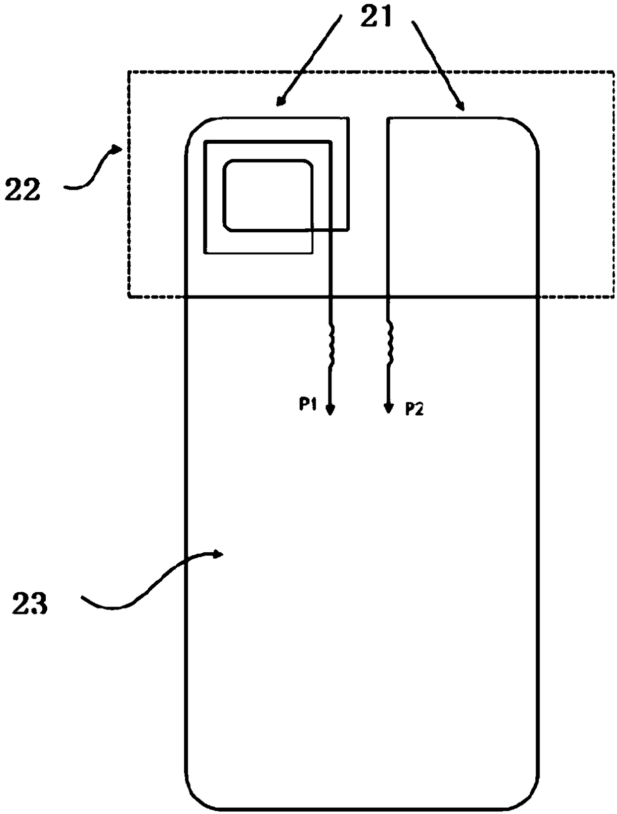
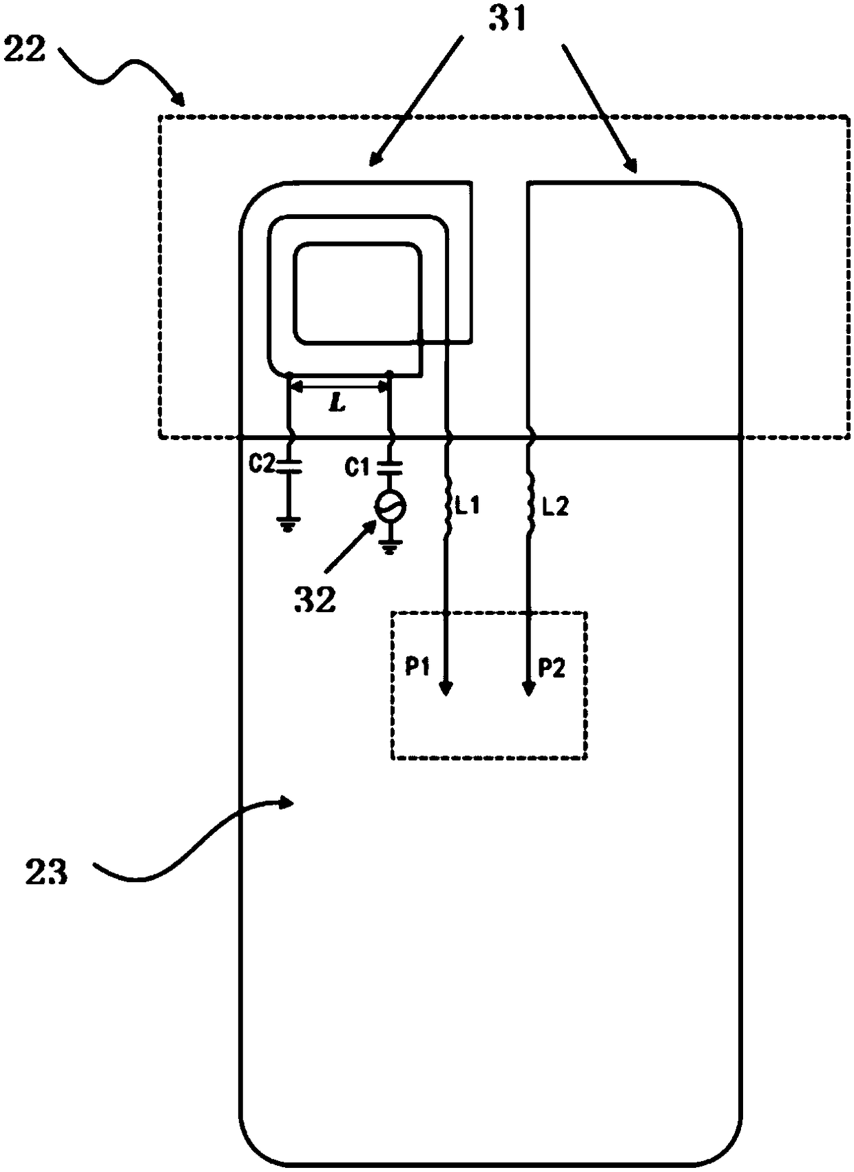
[0047] The invention discloses an electronic device, the structural diagram of which is as follows: figure 1 shown, including:

[0048] NFC coil 11 and first radio frequency feed point 12 .

[0049] The electronic device is a wireless communication electronic device, and has an antenna module, and an NFC antenna and the like are arranged on the antenna module.

[0050] Wherein, the NFC coil 11 serves as an NFC antenna of the electronic device.

[0051]The f...


PUM


Abstract

The invention discloses an electronic device and an antenna processing method. The electronic device comprises an NFC (near field communication) coil and a first radio frequency feed point arranged onthe NFC coil; the NFC coil is adopted as the NFC antenna of the electronic device; the first predetermined part metal of the NFC coil, which starts from the first radio frequency feed point and terminates at a radio frequency grounding point on the NFC coil constitutes a first loop antenna; and the first predetermined part metal on the NFC coil is used as the loop antenna of a first radio frequency band when the communication module of the electronic device operates in the first radio frequency band. According to the electronic device and the antenna processing method of the invention, the first radio frequency feed point is arranged on the NFC coil, so that the loop antenna operating in the first radio frequency band can be set on the NFC antenna; and the NFC antenna can be multiplexed,so that space occupied by the antenna can be decreased, and therefore, sufficient distances between the antennas in a limited space can be ensured, and signal interference between the antennas can bereduced.

Description

technical field [0001] The invention relates to the field of antennas, in particular to an electronic device and an antenna processing method. Background technique [0002] At present, some antennas in wireless communication electronic equipment are usually arranged in specific areas of the electronic equipment, such as: top area, side area. Antennas installed in the same clearance area of ​​electronic equipment antennas may include: hierarchical antennas, GPS antennas, cellular mobile communication main diversity, MIMO antennas, and various antennas such as Wifi2.4G / BT antennas and Wifi5G antennas. [0003] However, since the space of a specific area of ​​an electronic device is limited, various antennas are arranged in a specific area with limited space, which may easily cause signal interference between the antennas. Contents of the invention [0004] In view of this, the present invention provides an electronic device and an antenna processing method to solve the prob...

Claims


Application Information

Patent Timeline
IPC IPC(8): H01Q1/22H01Q7/00
CPCH01Q1/22H01Q7/00
Inventor 刘君英
Owner LENOVO (BEIJING) CO LTD
Why Eureka
Try Eureka