Array substrate, manufacturing method thereof, and touch display device

A technology of an array substrate and a manufacturing method, which is applied in the display field and can solve the problems of low visibility of a touch display device

Active Publication Date: 2020-12-29
BOE TECH GRP CO LTD +1
View PDF13 Cites 0 Cited by
  • Summary
  • Abstract
  • Description
  • Claims
  • Application Information

AI Technical Summary

Problems solved by technology

[0003] Embodiments of the present invention provide an array substrate, a manufacturing method thereof, and a touch display device, which can solve the problem of low visibility of the touch display device

Method used


Image

  • Array substrate, manufacturing method thereof, and touch display device
  • Array substrate, manufacturing method thereof, and touch display device
  • Array substrate, manufacturing method thereof, and touch display device

Examples


Embodiment Construction

[0032]The following will clearly and completely describe the technical solutions in the embodiments of the present invention with reference to the accompanying drawings in the embodiments of the present invention. Obviously, the described embodiments are only some, not all, embodiments of the present invention. Based on the embodiments of the present invention, all other embodiments obtained by persons of ordinary skill in the art without making creative efforts belong to the protection scope of the present invention.

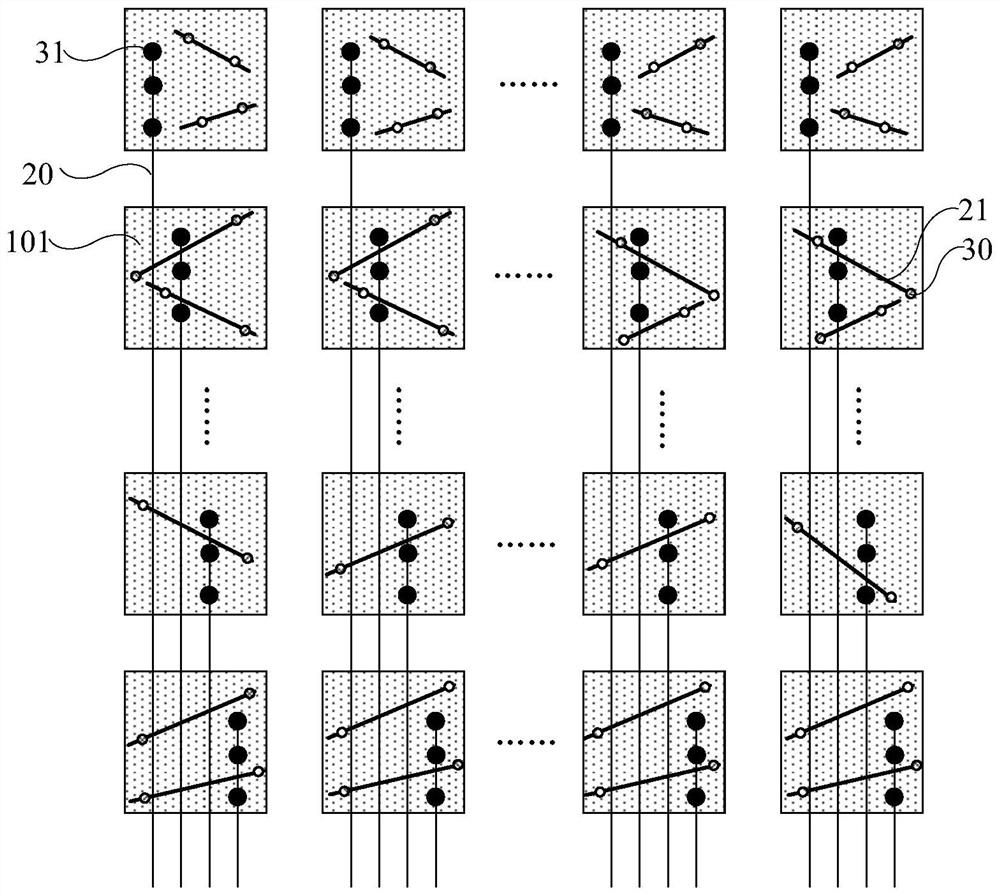
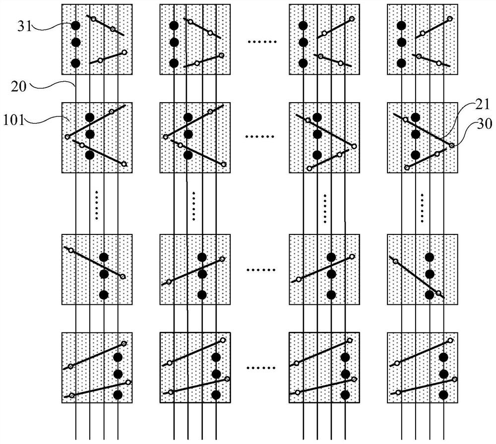
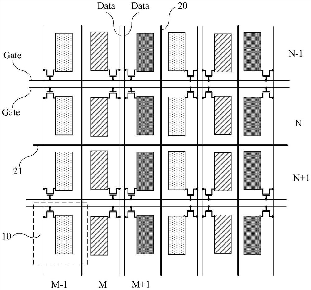
[0033] An embodiment of the present invention provides an array substrate, including a common electrode layer disposed on the base substrate 01 and such as figure 1 A plurality of touch leads 20 are shown.

[0034] Wherein, the common electrode layer includes a plurality of self-capacitance electrodes 101 insulated from each other and arranged in a matrix, and each touch lead 20 is electrically connected to one self-capacitance electrode 101 . Materials consti...


PUM


Abstract

Embodiments of the present invention provide an array substrate, a manufacturing method thereof, and a touch display device, which relate to the field of display technology and can solve the problem of low visibility of the touch display device. An embodiment of the present invention provides an array substrate including a common electrode layer and a plurality of touch leads arranged on the base substrate. The common electrode layer includes a plurality of self-capacitance electrodes insulated from each other and arranged in a matrix. Each touch lead It is electrically connected to a self-capacitance electrode; the array substrate also includes a plurality of suspension wires, the self-capacitance electrode is electrically connected to at least one suspension wire through at least two first via holes, and the orthographic projection of the suspension wire on the base substrate is located at the self- The capacitive electrodes are within the range of the orthographic projection on the substrate substrate. The above-mentioned array substrate is used for preparing a touch display device.

Description

technical field [0001] The present invention relates to the field of display technology, in particular to an array substrate, a manufacturing method thereof, and a touch display device. Background technique [0002] A touch display device is a common way of human-computer interaction. At present, the touch panel and the display panel of most touch devices are arranged independently, that is, the touch panel is arranged on the display side of the display panel. In this case, extraneous light is reflected on the upper surface of the display panel and the lower surface of the touch panel, thereby reducing the visibility of the display panel in brightly lit environments such as outdoors. Contents of the invention [0003] Embodiments of the present invention provide an array substrate, a manufacturing method thereof, and a touch display device, which can solve the problem of low visibility of the touch display device. [0004] In order to achieve the above object, embodiment...

Claims


Application Information

Patent Timeline
Patent Type & Authority Patents(China)
IPC IPC(8): G06F3/041G06F3/044
CPCG06F3/0412G06F3/044G06F2203/04111G06F2203/04103G06F3/04164G06F3/0443H10K59/40
Inventor 陶健李红敏唐锋景董职福薛伟
Owner BOE TECH GRP CO LTD
Why Eureka
Try Eureka