Method of attaching semiconductor material

A semiconductor and attachment technology, applied in semiconductor devices, semiconductor/solid-state device manufacturing, semiconductor/solid-state device testing/measurement, etc., to achieve the effects of improving accuracy, reducing defect images, and reliable image information

Pending Publication Date: 2019-04-12
HANMI SEMICON CO LTD
View PDF5 Cites 0 Cited by
  • Summary
  • Abstract
  • Description
  • Claims
  • Application Information

AI Technical Summary

Problems solved by technology

[0008] Therefore, although all materials entering into the viewing angle are inspected one by one in order to improve productivity, the mechanical error value of the attached table and vision camera has to be reflected in the accuracy

Method used


Image

  • Method of attaching semiconductor material
  • Method of attaching semiconductor material
  • Method of attaching semiconductor material

Examples


Embodiment Construction

[0045] Hereinafter, several preferred embodiments of the present invention will be described in detail with reference to the accompanying drawings. However, the invention is not limited to the embodiments described here, but can also be embodied in different ways. Rather, various embodiments described herein are provided so that the disclosure will be thorough and complete, and to fully convey the concept of the invention to those of ordinary skill in the art to which the invention pertains. Throughout the specification, the same reference numerals denote the same structural elements.

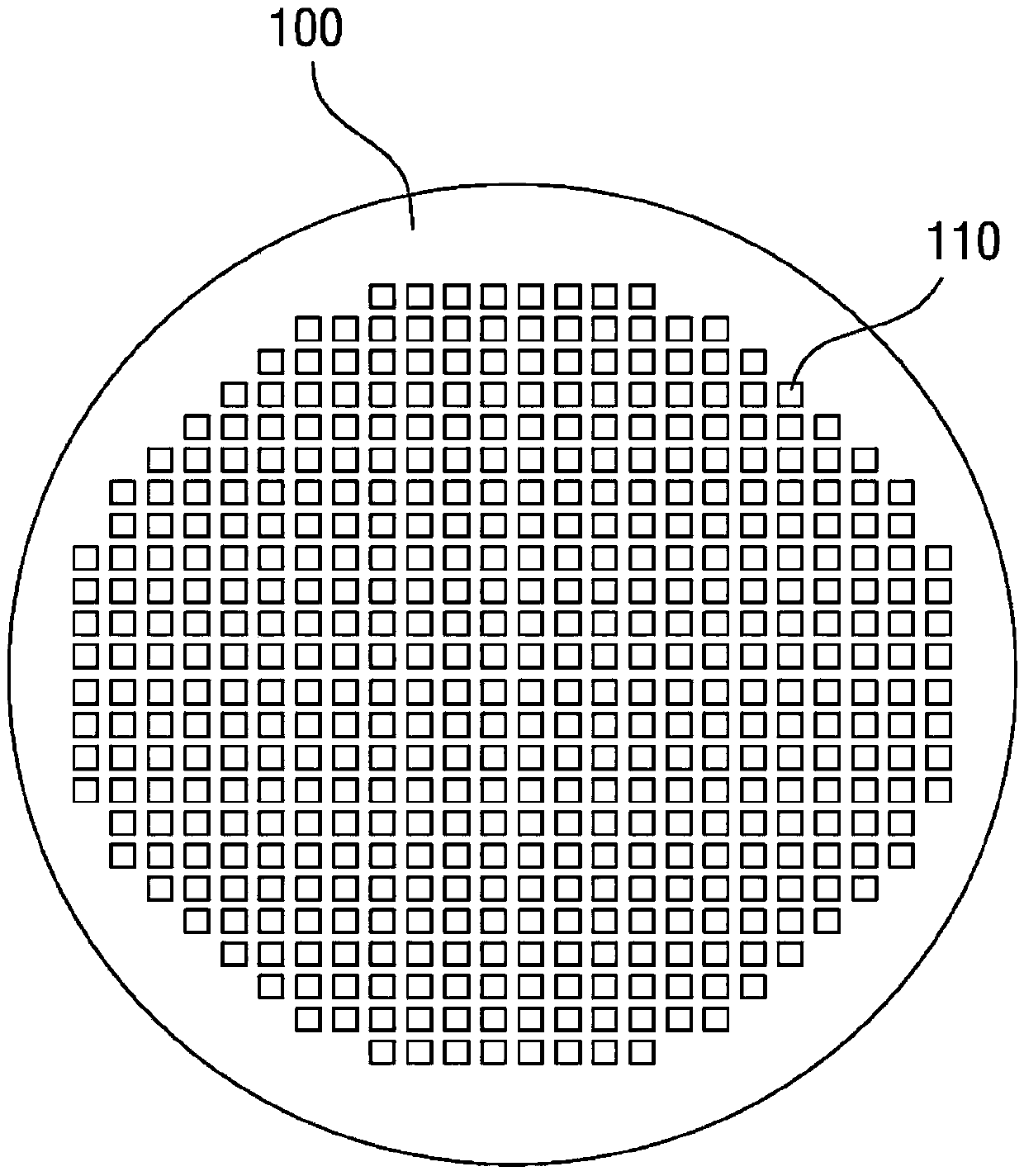
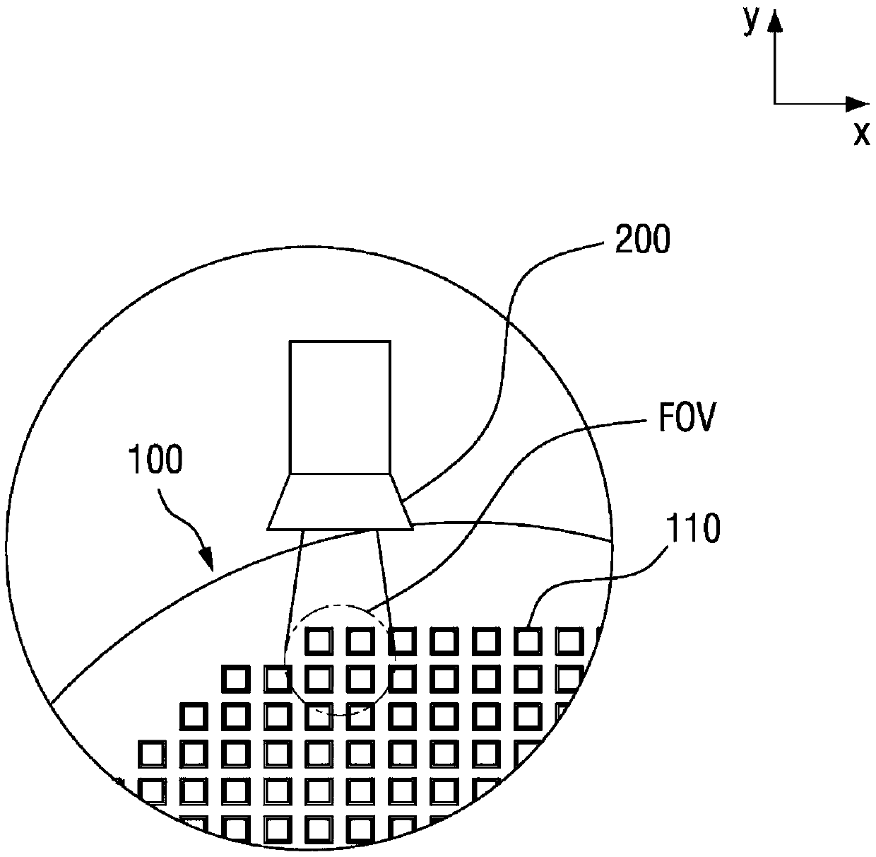
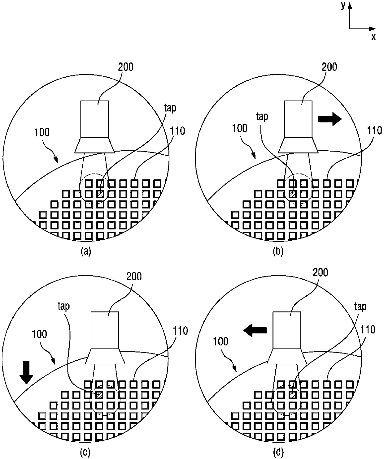
[0046] figure 1 To show a plan view of an attachment object 100 having a plurality of attachment positions 110 by picking up a semiconductor material and attaching a semiconductor material attachment device (attaching device) having an attachment unit according to the first embodiment of the present invention, figure 2 To show the state of photographing by the vision unit 200 in the first em...


PUM


Abstract

The present invention relates to a method for a semiconductor material attaching device to quickly and accurately correct the position error of an attaching position in a process of attaching a semiconductor material. According to the present invention, a vision or a table is shifted by an interval calculated according to the matrix information of a tagging area to be detected in the view angle ofthe vision unit, and a plurality of images in which the respective target sticking areas are at different positions And determines the position of the target touching area from the images.

Description

technical field [0001] The present invention relates to semiconductor material attachment methods. In more detail, the present invention relates to a method of attaching a semiconductor material attaching device (Semiconductor or Device Attaching Method) that improves inspection accuracy by accurately detecting the attachment position of the semiconductor material. Background technique [0002] In the semiconductor material attachment device, the individualized semiconductor material must first accurately grasp the preset attachment position of the attachment object in order to attach the attachment object for subsequent processes. [0003] Such attachment means may be adhesive means for bonding a plurality of semiconductor materials to a substrate, or attachment means for attaching to a tape for other subsequent processes. Also, there may be an attachment means for attaching the semiconductor material to the tape to accommodate spherical surfaces of the semiconductor mater...

Claims


Application Information

Patent Timeline
Patent Type & Authority Applications(China)
IPC IPC(8): H01L21/67H01L21/66H01L21/60
CPCH01L24/80H01L21/67144H01L21/67259H01L21/67294H01L22/20H01L2224/80122
Inventor 李暻植
Owner HANMI SEMICON CO LTD
Why Eureka
Try Eureka