Array substrate, manufacturing method thereof, and display device

A technology of array substrates and substrate substrates, applied in static indicators, instruments, nonlinear optics, etc., to achieve the effects of reducing interference, solving dark lines, and improving light transmittance

Active Publication Date: 2021-11-30
HKC CORP LTD +1
View PDF5 Cites 0 Cited by
  • Summary
  • Abstract
  • Description
  • Claims
  • Application Information

AI Technical Summary

Problems solved by technology

[0004] Based on this, it is necessary to provide an array substrate and its manufacturing method and display device for the problem of dark lines in PSVA pixel design

Method used


Image

  • Array substrate, manufacturing method thereof, and display device
  • Array substrate, manufacturing method thereof, and display device
  • Array substrate, manufacturing method thereof, and display device

Examples


Embodiment Construction

[0026] In order to make the above objects, features and advantages of the present invention more comprehensible, specific implementations of the present invention will be described in detail below in conjunction with the accompanying drawings. In the following description, numerous specific details are set forth in order to provide a thorough understanding of the present invention. However, the present invention can be implemented in many other ways different from those described here, and those skilled in the art can make similar improvements without departing from the connotation of the present invention, so the present invention is not limited by the specific implementations disclosed below.

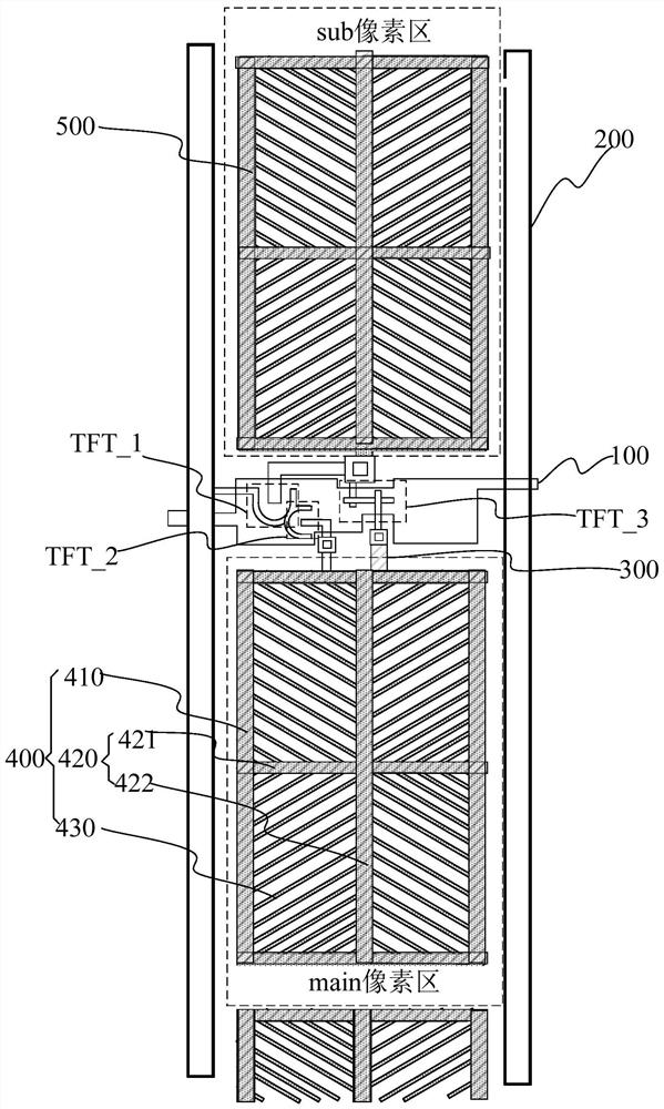
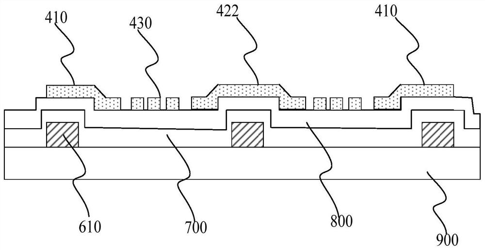
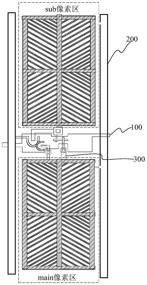
[0027] An embodiment of the present invention provides an array substrate, please refer to figure 1 with figure 2 , the array substrate includes a base substrate 900 and a scan line 100, a data line 200, a common electrode line 300 and a plurality of pixel units arranged on the base...


PUM


Abstract

Embodiments of the present invention provide an array substrate, a manufacturing method thereof, and a display device. The array substrate includes a base substrate and a scan line, a data line, a common electrode line and a plurality of pixel units arranged on the base substrate, and the pixel unit includes a thin film transistor, a main pixel electrode, a sub-pixel electrode and a common electrode. electrode, and at least one area between the main pixel electrode of the pixel unit and the sub-pixel electrode of the adjacent pixel unit is not provided with a common electrode, so as to reduce the voltage of the common electrode on the main pixel electrode and the pixel unit of the pixel unit. Interference in the area between the sub-pixel electrodes of adjacent pixel units, so as to solve the problem of dark lines caused by the disorder of liquid crystal orientation caused by the common electrode, improve the light transmittance in this area, and then improve the picture display quality .

Description

technical field [0001] The present invention relates to the field of display technology, in particular to an array substrate, a manufacturing method thereof, and a display device. Background technique [0002] Liquid Crystal Display (LCD) is one of the most widely used displays at present. LCD includes a pair of panels provided with field generating electrodes such as pixel electrodes and common electrodes and a liquid crystal layer arranged between the two panels. A voltage is applied to the field generating electrode to generate an electric field in the liquid crystal layer, and the liquid crystal molecules are deflected under the action of the electric field, so that the transmission of light can be controlled to make the LCD display images. Liquid crystal displays include twisted nematic (Twisted Nematic, TN) mode, electronically controlled birefringence (Electrically Controlled Birefringence, ECB) mode, vertical alignment (Vertical Alignment, VA) mode, etc. , wide view...

Claims


Application Information

Patent Timeline
Patent Type & Authority Patents(China)
IPC IPC(8): G02F1/133G02F1/1343G02F1/1362G09G3/36
CPCG02F1/136286G02F1/134309G02F1/13306G09G3/3685G09G3/3696G09G3/3648
Inventor 杨艳娜
Owner HKC CORP LTD
Why Eureka
Try Eureka