High voltage generator in semiconductor memory device

a high-voltage generator and memory device technology, applied in the direction of dc-dc conversion, digital storage, power conversion systems, etc., can solve the problems of unguaranteed osc of the last period of the pumping clock signal, relatively slow operation speed of the nmos transistor, etc., to increase the efficiency and duty of the charge pump

Active Publication Date: 2006-10-17
SK HYNIX INC
View PDF11 Cites 13 Cited by
  • Summary
  • Abstract
  • Description
  • Claims
  • Application Information

AI Technical Summary

Benefits of technology

[0012]It is, therefore, an object of the present invention to provide a semiconductor memory device having a high voltage generator for increasing efficiency and duty of a charge pump by guaranteeing an activation period of the charge pump.

Problems solved by technology

However, the NMOS transistor can fast transmit a logic low level data, i.e., ‘0’; but, in case of a logic high level data, i.e., ‘1’, an operating speed of the NMOS transistor is relatively slow because of a threshold voltage Vth.
However, referring to FIG. 2, if the oscillator enable signal OSCEN is inactivated, i.e., becomes a logic low level, the last period of the pumping clock signal OSC is not guaranteed.

Method used


Image

  • High voltage generator in semiconductor memory device
  • High voltage generator in semiconductor memory device
  • High voltage generator in semiconductor memory device

Examples


Embodiment Construction

[0020]Hereinafter, a high voltage generator included in a semiconductor memory device for increasing efficiency and duty of a charge pump according to the present invention will be described in detail referring to the accompanying drawings.

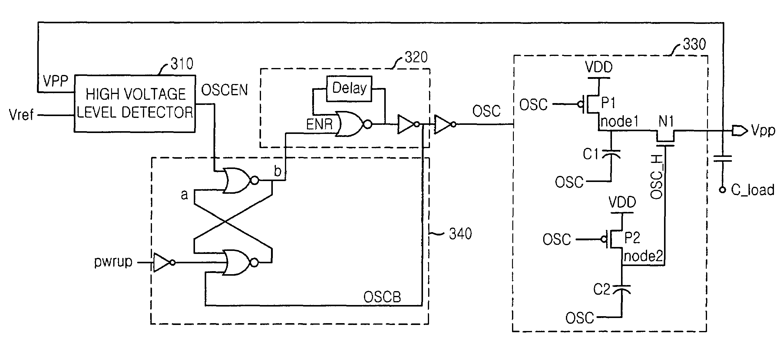
[0021]FIG. 3 is a block diagram showing a high voltage generator in a semiconductor memory device in accordance with the present invention.

[0022]As shown, the high voltage generator includes a high voltage level detector 310, an oscillator 320, a clock feedback block 340 and a charge pumping block 330.

[0023]The high voltage level detector 310 compares a high voltage VPP with a reference voltage Vref and generates an oscillator control signal OSCEN in response to a comparison result. Herein, the oscillator control signal OSCEN becomes a logic high level “H” if the high voltage VPP is under a predetermined level. That is, the oscillator control signal OSCEN outputted from the high voltage level detector 310 becomes a logic low level if the high volt...


PUM


Abstract

A high voltage generator includes a high voltage level detector for comparing a boosted high voltage with a reference voltage and generating an oscillator control signal being a first logic level in response to a comparison result; a clock feedback block for receiving the oscillator control signal and an inverse pumping control signal and keeping an oscillator enable signal in the first logic level for a predetermined period; an oscillator for generating a pumping control signal in response to the oscillator enable signal and outputting the inverse pumping control signal to the clock feedback block, wherein the pumping control signal is periodically toggled; and a charge pumping block for generating the boosted high voltage in response to the pumping control signal.

Description

FIELD OF INVENTION[0001]The present invention relates to a voltage generator for boosting a supply voltage; and, more particularly, to a high voltage generator included in a semiconductor memory device for raising a supply voltage to a predetermined level.DESCRIPTION OF PRIOR ART[0002]Recently, a supply voltage used in a semiconductor memory device becomes lower, but an operating speed of the semiconductor memory device becomes much faster. Thus, the semiconductor memory device boosts a supply voltage to a predetermined level for guaranteeing a stable operation and improves a speed for sensing a data in a unit cell.[0003]For example, in case of a dynamic random access memory (DRAM) of which unit cell is constituted with one capacitor and a transistor, the transistor in the unit cell is usually a NMOS transistor instead of a PMOS transistor because a size of the PMOS transistor is higher than that of the NMOS transistor. However, the NMOS transistor can fast transmit a logic low leve...

Claims


Application Information

Patent Timeline
Patent Type & AuthorityPatents(United States)
IPC IPC(8): G05F1/575H02M3/07G05F1/10G11C5/14G11C11/407
CPCG11C5/145G11C5/14
InventorDO, CHANG-HO
OwnerSK HYNIX INC