Supercharge Your Innovation With Domain-Expert AI Agents!

Trimming functional parameters in integrated circuits

a technology of functional parameters and integrated circuits, applied in the direction of electric variable regulation, process and machine control, instruments, etc., can solve the problems of several of the produced ic samples having to be discarded, and the implementation of functional parameters trimming in ics that is known to have problems,

Active Publication Date: 2007-05-22
MICRON TECH INC
View PDF7 Cites 1 Cited by
  • Summary
  • Abstract
  • Description
  • Claims
  • Application Information

AI Technical Summary

Problems solved by technology

Producing an IC is a very complex task, which involves several phases.
As a consequence to this unavoidable, statistical variations in the IC functional parameters, several of the produced IC samples might have to be discarded because they do not respect the intended specifications.
In the Applicant's opinion, the known implementations of the functional parameters trimming in ICs exhibit some problems.
A problem of the known solutions is that, being the trimmable circuit structures that exploit the bandgap reference voltage, namely the voltage regulators, normally uncorrelated from each other, it is necessary to trim each circuit block individually, with a significant waste of time.
In particular, the IC testing time suffers from a significant impact due to the trimming of all the trimmable circuit structures.
Measuring the bandgap reference voltage value is also a source of other problems.
However, due to the presence of parasitic elements (e.g., inductances of the bonding leads that connect the IC pads to the IC package pins, parasitic inductances of the printed circuit board on which the IC is mounted, and the like), the voltage levels on the IC pads are far from ideal, and are affected by overshoots / undershoots over / below the supply voltage VDD / the reference voltage GND.
Furthermore, when the voltage at the IC pad goes negative, the bulk-drain PN junction of the pass MOSFET is forwardly biased, and thus a relatively high current (of the order of the milliampere) is sunk from the bulk; this causes an unnecessary and undesired current consumption, especially in stand-by or power-down modes.
An additional problem that the Applicant has observed relates to the propagation of disturbances at the IC pad to the output node of the bandgap reference voltage generator, through the source-drain parasitic capacitance of the pass MOSFET, and also the propagation of disturbances from the gate of the pass MOSFET, to the output of the bandgap voltage generator, through the gate-source parasitic capacitance thereof.
Dual problems are encountered in case a P-channel pass MOSFET is used, in substitution of the N-channel one: in this case, the problems derive from voltage overshoots at the IC pad.
All these problems may greatly impair the correct functionality of the bandgap reference voltage generator and, as a consequence, of the whole IC.

Method used


Image

  • Trimming functional parameters in integrated circuits
  • Trimming functional parameters in integrated circuits
  • Trimming functional parameters in integrated circuits

Examples


Embodiment Construction

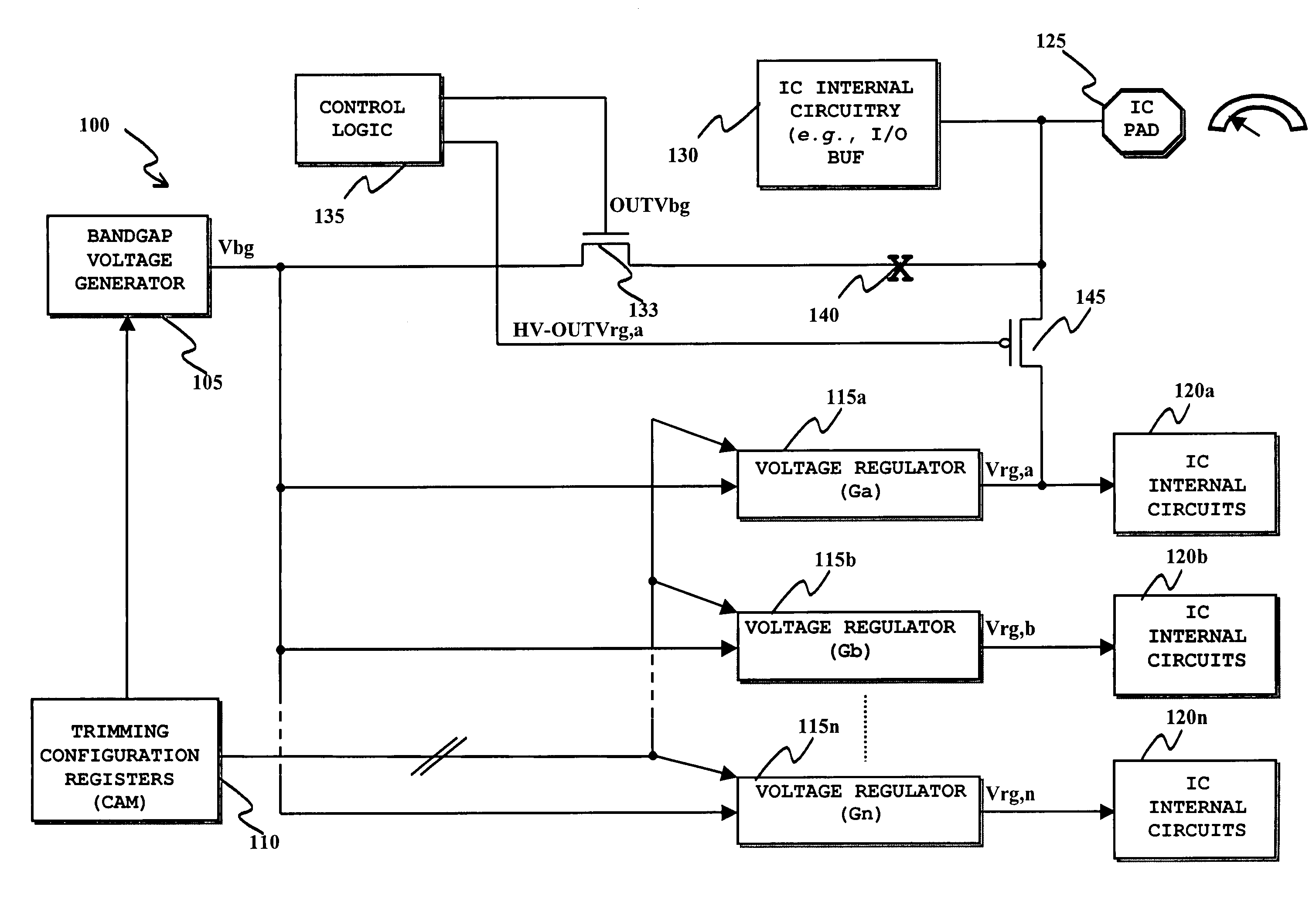
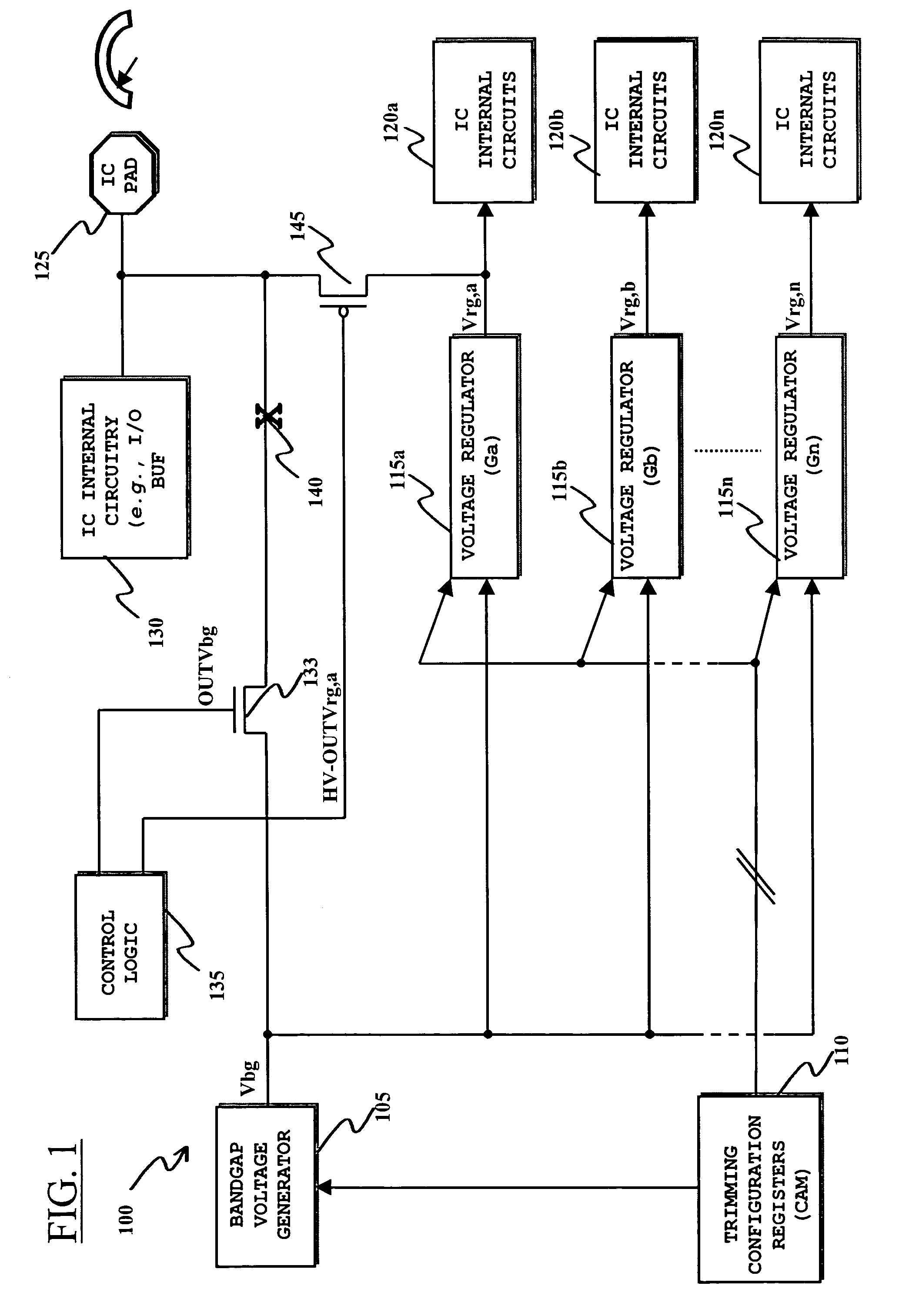
[0040]Making reference to the drawings, FIG. 1 schematically shows, in a generic IC identified as 100, the functional blocks relevant to the understanding of the invention embodiment to be described.

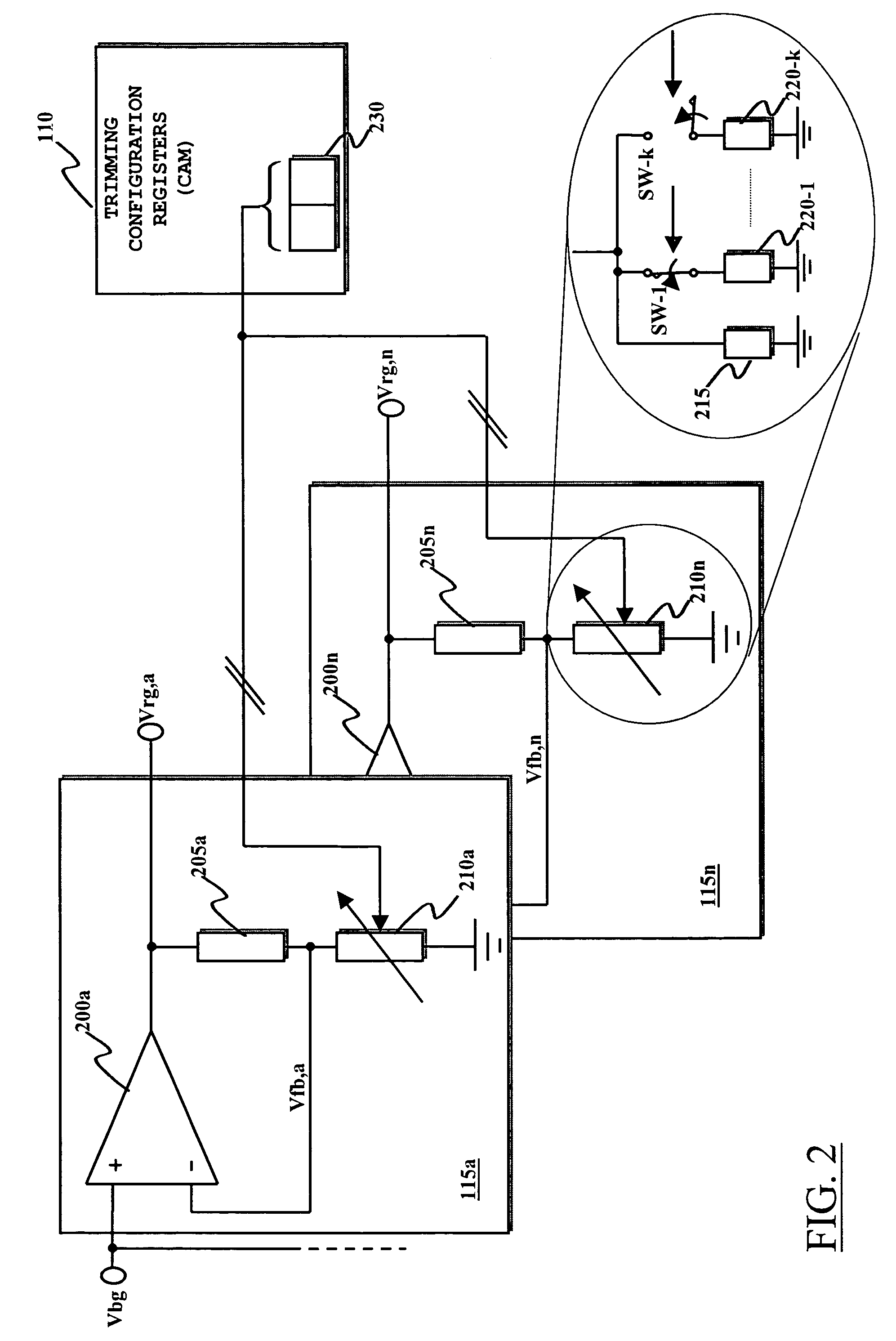
[0041]In particular, reference numeral 105 identifies a bandgap reference voltage generator, of the type frequently used in ICs for generating a voltage (the bandgap voltage) Vbg, stable against variations in temperature, used within the IC as a reference voltage for, e.g., generating other voltages or currents, and / or regulating the generated voltages / currents.

[0042]The value Vbg of the bandgap voltage Vbg can be expressed as a function of the base-emitter voltage Vbe of a bipolar junction transistor, and of the thermal voltage VT:

Vbg=Vbe+G*VT,

where the value of the factor G determines the compensation in temperature of the voltage Vbe.

[0043]The detailed structure of the bandgap reference voltage generator 105 is not depicted in detail, being a circuit per-se well known in the art and, ...


PUM


Abstract

A trimming structure for trimming functional parameters of an Integrated Circuit—IC—(100) includes a first (115a) and at least one second functional blocks (115b, . . . ,115n) with which a first (Vrg,a) and at least one second IC functional parameters (Vrg,b, . . . ,Vrg,n) are respectively associated. The trimming structure includes respective trimmable circuit structures (205a,210a, . . . ,205n,210n) included in the first and at least one second functional blocks, and trimming configuration storage (110) for storing trimming configurations for the trimmable circuit structures. A change in the trimming configuration of the first functional block causes a corresponding change in the trimming configuration of the second functional block. Further, a change in the second IC functional parameter in response to the corresponding change in the trimming configuration of the second functional block is proportional to the change in the first IC functional parameter consequent to the change in the trimming configuration of the first functional block.

Description

CROSS-REFERENCE TO RELATED APPLICATION[0001]This application is based upon and claims priority from prior European Patent Application No. EP04101718.7, filed on 26 Apr. 2004, the entire disclosure of which is herein incorporated by reference.BACKGROUND OF THE INVENTION[0002]1. Field of the Invention[0003]The present invention relates in general to the field of Integrated Circuits (ICs). Specifically, the invention concerns trimming methods, and related structures, adapted to allowing the implementation of functional parameters adjustment in ICs.[0004]2. Description of the Related Art[0005]Producing an IC is a very complex task, which involves several phases. In very general terms, starting for example from the IC architectural design, the different electronic circuits / circuit blocks are designed and simulated by means of CAD tools, then the physical layout of the several different IC layers is defined and the photolithographic masks necessary for the planar technology manufacturing ...

Claims


Application Information

Patent Timeline
Patent Type & Authority Patents(United States)
IPC IPC(8): G05F1/10G05F3/02G05F3/30G11C5/14G11C29/02H03H11/26
CPCG11C5/147G11C29/02G11C29/021G11C29/028
Inventor CRIPPA, LUCASANGALLI, MIRIAMSCOMMEGNA, SALVATRICEMICHELONI, RINO
Owner MICRON TECH INC
Features
  • R&D
  • Intellectual Property
  • Life Sciences
  • Materials
  • Tech Scout
  • Unparalleled Data Quality
  • Higher Quality Content
  • 60% Fewer Hallucinations
Learn More