Plasma display device

a technology of plasma and display device, which is applied in the direction of static indicating device, address electrode, instrument, etc., can solve the problem of lowering the image contrast, and achieve the effect of prolonging the voltage range as a margin for proper discharge, preventing from causing erroneous discharge, and improving contras

Inactive Publication Date: 2010-08-31
PANASONIC CORP
View PDF15 Cites 4 Cited by
  • Summary
  • Abstract
  • Description
  • Claims
  • Application Information

AI Technical Summary

Benefits of technology

[0012]It is an object of the present invention is to provide a plasma display device and a plasma display panel driving method which are capable of improving image contrast while preventing from causing erroneous discharge.
[0015]In the plasma display device and the plasma display panel driving method according to the present invention, the two other sustain pulses, which have rise timings different from each other by a predetermined period of time and have partly overlapping application periods, are applied to row electrodes forming each of the row electrode pairs after ending of the sustain period in one subfield of the one-field display period, so that erasure discharge is generated in the discharge cells where sustain discharge has been caused in the one subfield. This allows to set all the discharge cells into a uniform wall charge state, by the reset discharge in the beginning subfield of the next field. Namely, the erasure discharge can make uniform the wall charge states in discharge cells which have emitted light and the other discharge cells which have not emitted light in the last subfield of the preceding field. Accordingly, a voltage range as a margin for proper discharge can be extended thus improving the contrast while preventing from causing erroneous discharge. Further, since a narrow-width pulse for the erasure discharge is equivalently produced by applying the different sustain pulses deviated from each other by the predetermined period of time in rise timing, it is unnecessary to form a structure for especially producing the narrow-width erasure discharge pulse.

Problems solved by technology

Thus, there is a problem that image contrast is lowered since the light emission occurs regardless of pixel data at six points shown by hatching in FIG. 1.

Method used


Image

  • Plasma display device
  • Plasma display device
  • Plasma display device

Examples


Embodiment Construction

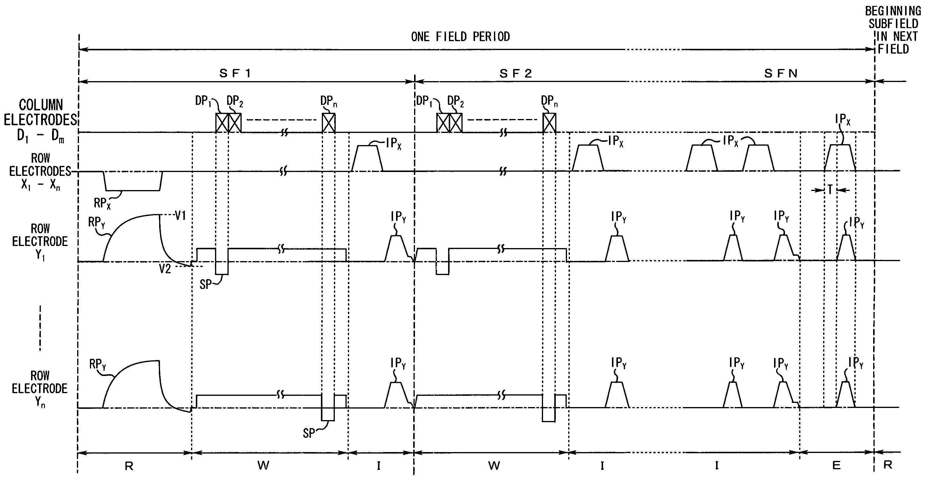
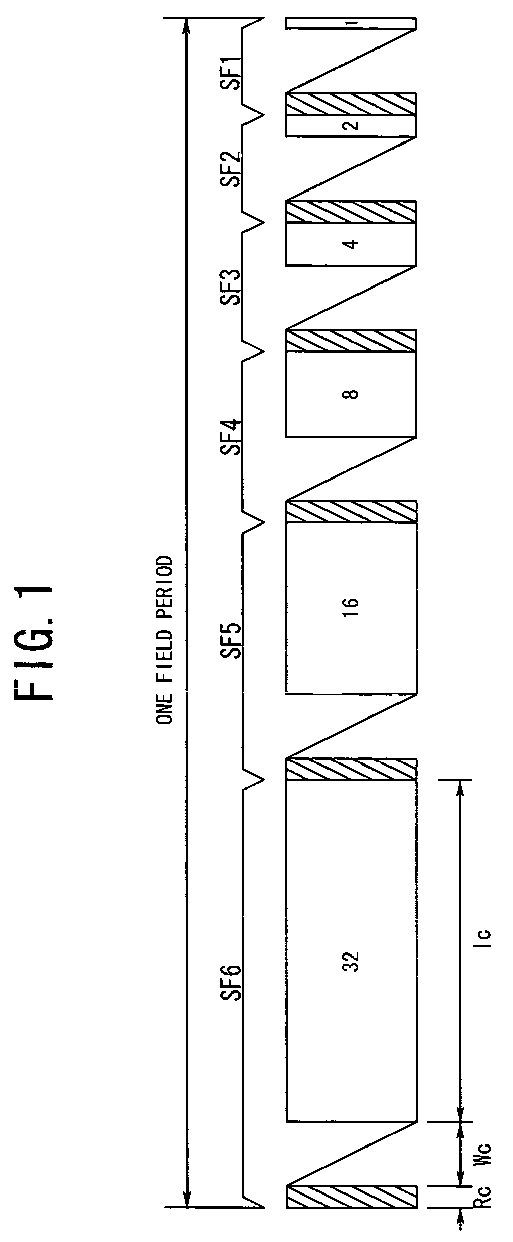
[0031]Hereinafter, an embodiment according to the present invention will be described in detail with reference to the drawings.

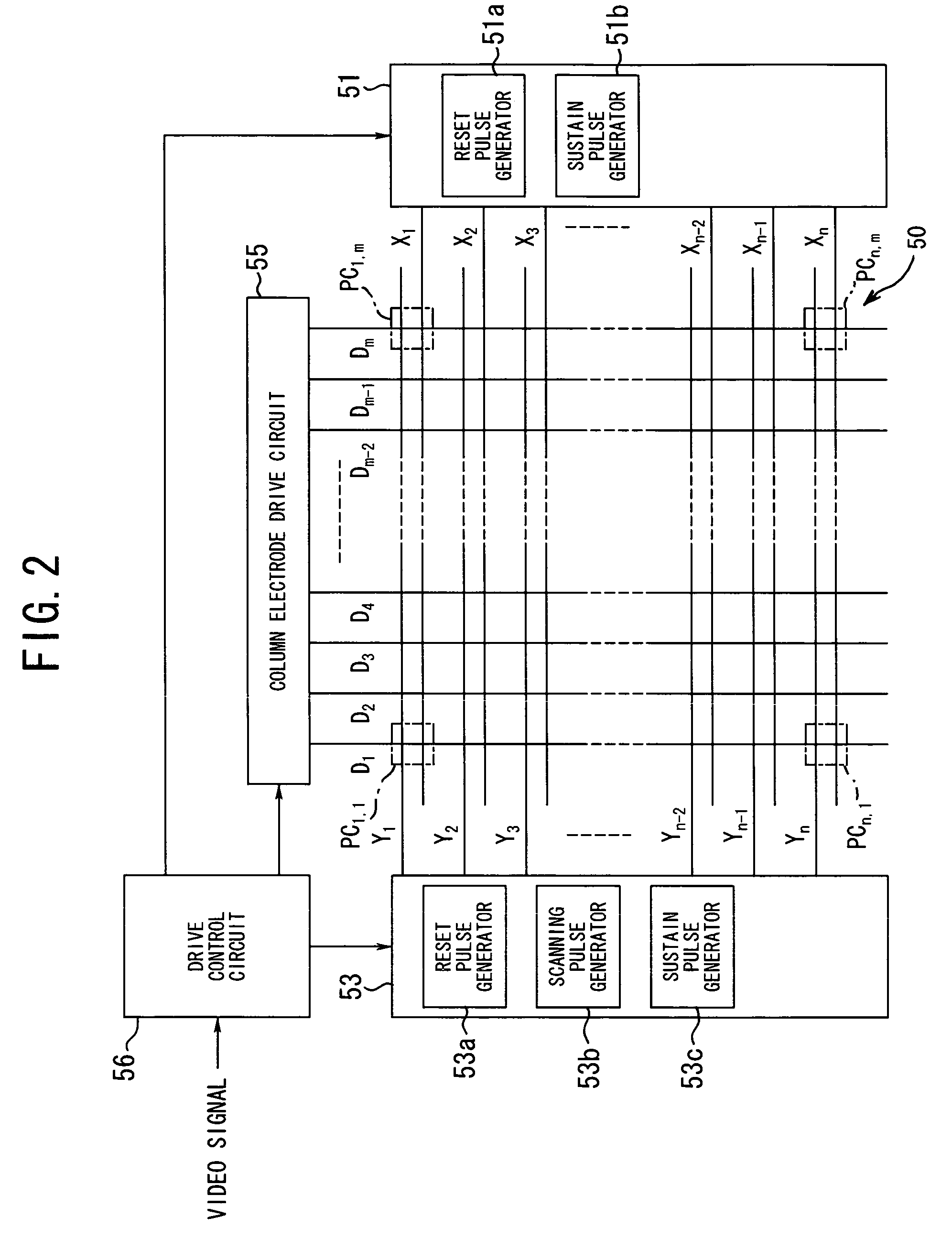
[0032]FIG. 2 is a diagram illustrating an outline configuration of a plasma display device according to the invention.

[0033]As shown in FIG. 2, the plasma display device is configured of a PDP 50 as a plasma display panel, an X-row electrode drive circuit 51, a Y-row electrode drive circuit 53, a column electrode drive circuit 55, and a drive control circuit 56.

[0034]In the PDP 50, column electrodes D1 to Dm are extended and arranged in the longitudinal direction (vertical direction) of a two-dimensional display screen, and row electrodes X1 to Xn and row electrodes Y1 to Yn are extended and arranged in the lateral direction (the horizontal direction) thereof. The row electrodes X1 to Xn and row electrodes Y1 to Yn form row electrodes pairs (Y1, X1), (Y2, X2), (Y3, X3), . . . , (Yn, Xn) which are paired with those adjacent to each other and which serve as th...


PUM


Abstract

A plasma display device which generates reset discharge in a reset period prior to an address period in the beginning subfields of a one-field display period, and applies two sustain pulses, which have rising timings different from each other by a predetermined period of time and have partly overlapping application periods, to row electrodes forming each row electrode pair after ending a sustain period in a last subfield of the one-field display period to thereby cause erasure discharge in discharge cells where sustain discharge has been caused in the last subfield.

Description

BACKGROUND OF THE INVENTION[0001]1. Field of the Invention[0002]The present invention relates to a plasma display device using a plasma display panel.[0003]2. Description of the Related Background Art[0004]There is known an AC (alternating current) type PDP (plasma display panel) as one display panel in a scheme of matrix display. The AC type PDP has a plurality of column electrodes (address electrodes) and a plurality of row electrode pairs which are arranged orthogonal to the column electrodes and which each form a scanning line. Each of the row electrode pairs and each of the column electrodes are covered by a dielectric layer for a discharge space, providing a structure forming a discharge cell, corresponding to one pixel, at an intersection of each of the row electrode pairs and each of the column electrodes.[0005]Here, there is so-called a subfield method in which one field period is divided into N subfields to perform light emission for a time period corresponding to weightin...

Claims


Application Information

Patent Timeline
Patent Type & Authority Patents(United States)
IPC IPC(8): G09G3/28G09G3/20G09G3/292G09G3/288G09G3/291G09G3/294G09G3/296G09G3/298H01J11/12H01J11/22H01J11/24H01J11/26H01J11/34H01J11/36H01J11/38H01J11/40H01J11/42H01J11/44
CPCG09G3/2927G09G3/2922G09G2310/066G09G2320/0238H01J2211/40
Inventor SAKATA, KAZUAKI
Owner PANASONIC CORP
Why Eureka
Try Eureka