Optoelectronic device, use of a dual emitter as wavelength conversion material

a technology of optical equipment and wavelength conversion material, which is applied in the direction of light and heating equipment, organic chemistry, spectral modifiers, etc., can solve the problems of reducing the efficiency of wavelength conversion and achieve the effect of higher luminous efficacy

Active Publication Date: 2018-04-24
OSRAM OLED
View PDF14 Cites 6 Cited by
  • Summary
  • Abstract
  • Description
  • Claims
  • Application Information

AI Technical Summary

Benefits of technology

[0006]Embodiments of the invention provide an optoelectronic apparatus which permits a higher efficiency, in particular, higher efficiency of wavelength conversion.

Problems solved by technology

In particular, reabsorption of radiation, for example, of secondary radiation which has already been formed by conversion, can distinctly reduce the efficiency of wavelength conversion.

Method used


Image

  • Optoelectronic device, use of a dual emitter as wavelength conversion material
  • Optoelectronic device, use of a dual emitter as wavelength conversion material
  • Optoelectronic device, use of a dual emitter as wavelength conversion material

Examples


Embodiment Construction

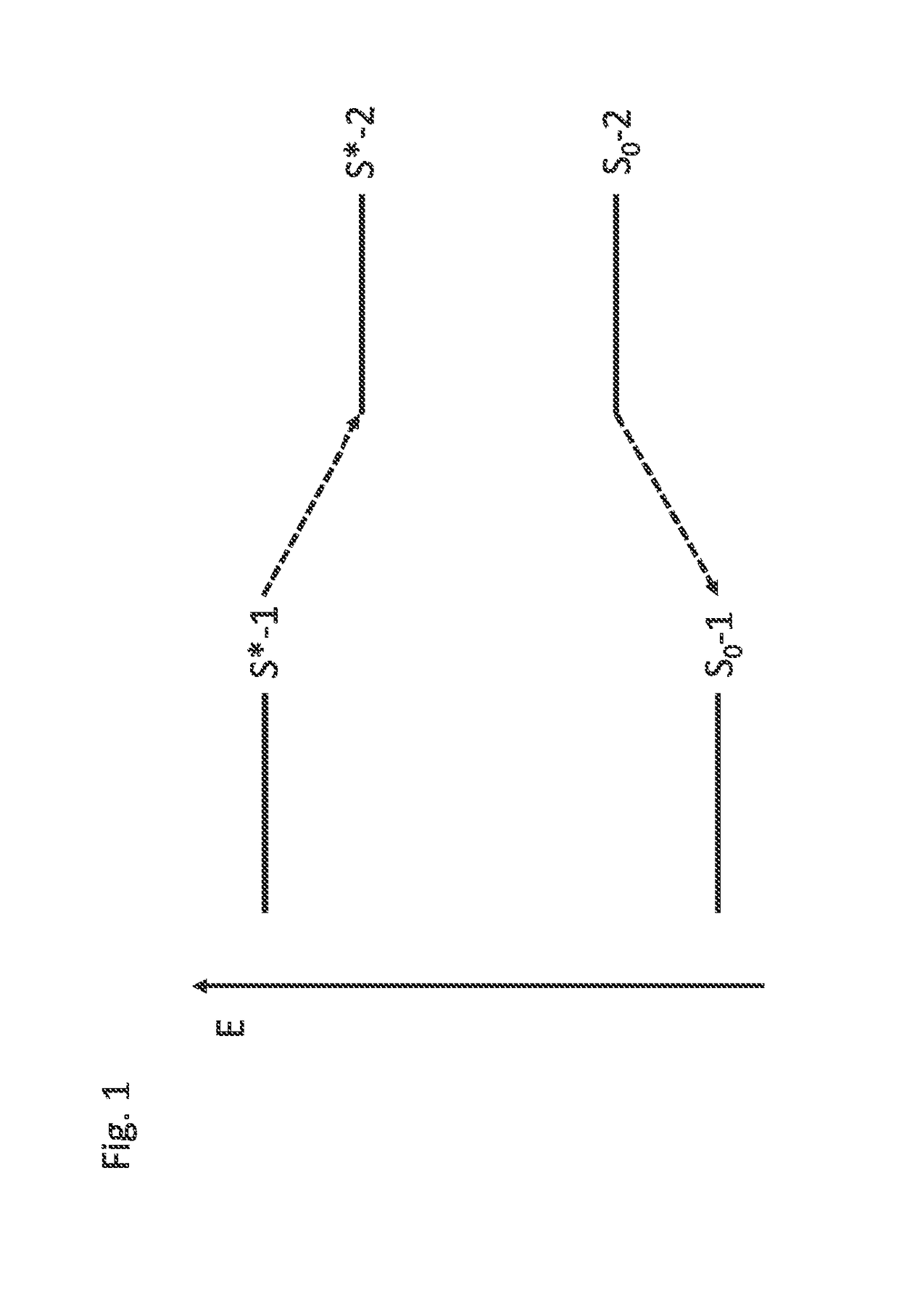
[0162]FIG. 1 shows the energy level diagram for a dual emitter, wherein E denotes the energy of the electronic states. Absorption of a photon induces an electronic transition from the first electronic base state (So-1) into the first electronically excited state (S*-1). A transition from the first electronically excited state (S*-1) into the second electronically excited state (S*-2) then occurs. This transition may proceed, for example, by means of intramolecular charge transfer or intramolecular proton transfer. The dual emitter is in principle capable of emitting radiation from both electronically excited states. If the transition proceeding from the first electronically excited state (S*-1) into the second electronically excited state (S*-2) proceeds faster than the radiant transition from the first electronically excited state (S*-1) into the first electronic base state (So-1), emission may mainly proceed from the second electronically excited state (S*-2). Since the reverse re...


PUM

PropertyMeasurementUnit
molecular weightaaaaaaaaaa
thicknessaaaaaaaaaa
thicknessaaaaaaaaaa

Abstract

An optoelectronic apparatus is disclosed. In an embodiment, the apparatus includes at least one wavelength conversion region which includes at least one dual emitter as wavelength conversion material, wherein the wavelength conversion region converts primary radiation at least in part into secondary radiation, and wherein the dual emitter includes a first electronic base state and a second electronic base state, together with a first electronically excited state and a second electronically excited state which may be reached from the first electronically excited state. The dual emitter further includes emission proceeding from the second electronically excited state into the second base state.

Description

[0001]This patent application is a national phase filing under section 371 of PCT / EP2015 / 076228, filed Nov. 10, 2015, which claims the priority of German patent application 10 2014 116 613.2, filed Nov. 13, 2014, each of which is incorporated herein by reference in its entirety.TECHNICAL FIELD[0002]The present invention relates to an optoelectronic apparatus and to the use of a dual emitter as wavelength conversion material.BACKGROUND[0003]Optoelectronic apparatuses such as, for example, light-emitting diodes (LEDs), for example, organic light-emitting diodes (OLEDs), organic lasers such as, for example, surface emitters (“VCSELs”, vertical cavity surface emitting lasers) as well as solar cells or photodetectors may comprise wavelength conversion regions which convert primary radiation into secondary radiation.[0004]The efficiency of optoelectronic apparatuses depends inter alia on how effectively the primary radiation is converted into secondary radiation and the extent to which lo...

Claims


Application Information

Patent Timeline
Patent Type & Authority Patents(United States)
IPC IPC(8): H01L33/50C07C211/48C07D209/08F21V9/40
CPCH01L33/502C07D209/08C07C211/48H10K59/38H10K50/125H01L33/50H10K85/615H10K85/6572
Inventor PENTLEHNER, DOMINIK
Owner OSRAM OLED
Why Eureka
Try Eureka