
Polishing pad with controlled void formation
A polishing pad and pore technology, applied in the fields of chemical mechanical planarization polishing pads and semiconductor devices
Patent Information
- Authority / Receiving Office
- CN · China
- Patent Type
- Patents(China)
- Current Assignee / Owner
- Publication Date
- 2013-10-16
- Estimated Expiration
- Not applicable · inactive patent
Smart Images
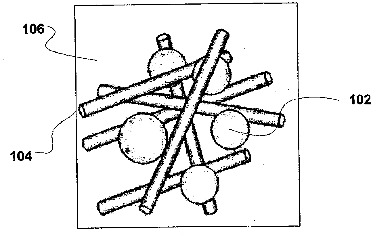
Figure 1 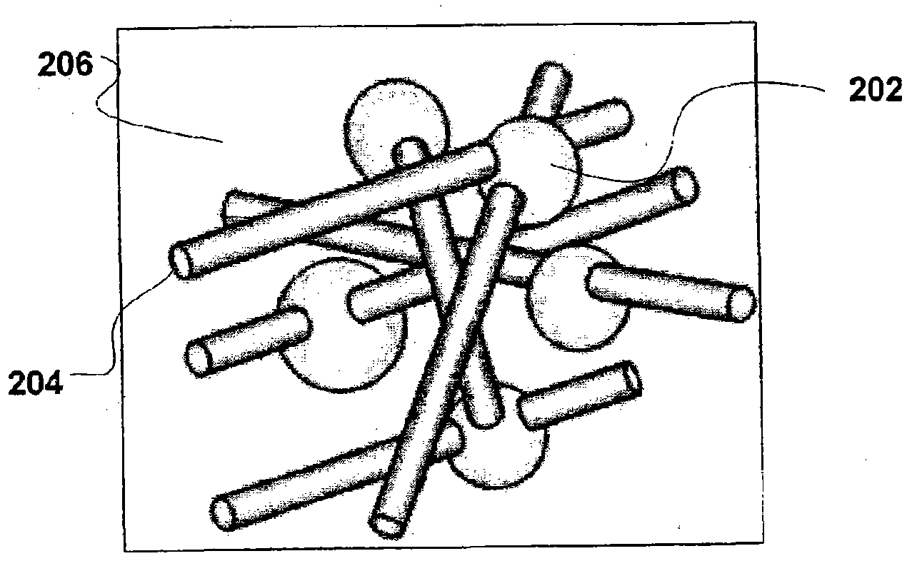
Figure 2 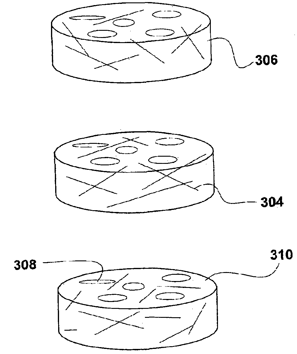
Figure 3
Abstract
Description
[0001] Related Application Cross Reference
[0002] This application claims priority based on US Provisional Patent Application Serial No. 61 / 041,422, filed April 1, 2008, which is hereby incorporated by reference in its entirety. technical field
[0003] The present invention relates to a chemical / mechanical polishing pad for polishing materials, such as for semiconductor devices formed from relatively flat or thin semiconductor materials such as silicon. The polishing pad may comprise a fibrous polymer matrix containing pores, wherein the pore geometry, distribution, size, etc. are adjusted to target levels by manufacturing protocols. Background technique
[0004] When chemical mechanical planarization (Chemical Mechanical Planarization; CMP) is used as a process step in the manufacture of microelectronic devices such as semiconductor wafers, blanket silicon wafers (blanket silicon wafer) and computer hard disks, the polishing pad can be mixed with abrasive or A non-ab...
Examples
Embodiment Construction
[0025] It should be understood that the disclosure of the invention is not limited in its application to the details of construction and the arrangement of elements described in the following description and shown in the drawings. The embodiments herein are capable of other embodiments and of being practiced or carried out in various ways. It is also to be understood that the phraseology and terminology employed herein are for the purpose of description and should not be regarded as limiting. As used herein, "comprising", "comprising" or "having" and variations thereof are meant to encompass the items listed thereafter and their equivalents as well as others. Unless otherwise limited, the terms "connected," "coupled," and "mounted" and variations thereof herein are used broadly and include both direct and indirect connections, couplings, and mountings. Additionally, the terms "connected," "coupled," and variations thereof are not limited to physical or mechanical connections ...