
Manufacturing method of large-power vertical light-emitting diode
A technology of light-emitting diodes and manufacturing methods, applied in semiconductor/solid-state device manufacturing, electrical components, circuits, etc., can solve problems such as cracking of metal sapphire substrates, increase of production costs, and reduction of core particle yield, so as to facilitate separation, The effect of reducing warpage and reducing difficulty
Patent Information
- Authority / Receiving Office
- CN · China
- Patent Type
- Applications(China)
- Current Assignee / Owner
- Publication Date
- 2012-07-04
Smart Images
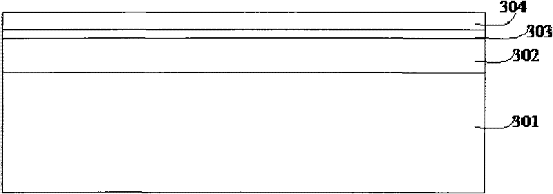
Figure 1 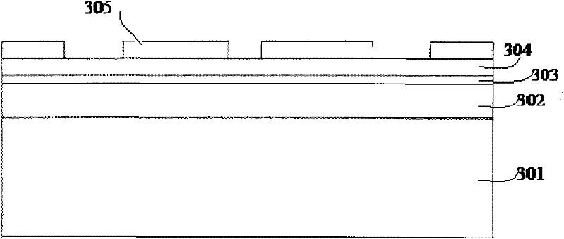
Figure 2 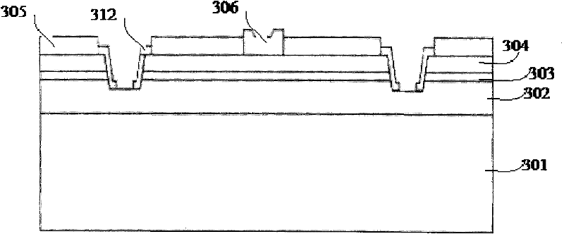
Figure 3
Abstract
Description
technical field
[0001] The invention relates to the technical field of manufacturing semiconductor optoelectronic devices, in particular to a method for manufacturing a GaN-based high-power vertical structure LED chip. Background technique
[0002] As a solid-state lighting source, GaN-based LEDs have the advantages of high photoelectric conversion efficiency, environmental protection, long life, and fast response. With the development and application of GaN-based high-brightness LEDs, a new generation of green and environmentally friendly solid-state lighting sources GaN-based LEDs has become the focus of attention. Since the sapphire substrate used for growth is non-conductive, traditional GaN-based LEDs use a planar electrode structure, with both p-type and n-type contact electrodes on the upper surface, and n-type electrodes are prepared by etching to n-type by photolithography-etching. Front-mount LEDs have a simple structure and are easy to process, but because the st...
Examples
Embodiment Construction
[0028] Method steps of the present invention are:
[0029] 1) see figure 1 , growing an N-type GaN-based semiconductor layer 302, a quantum well active region 303, and a P-type GaN-based semiconductor layer 304 sequentially on the sapphire substrate 301 by metal-organic chemical vapor deposition;
[0030] 2) see figure 2 , on the P-type GaN-based semiconductor layer 304, a reflective metal layer 305 is evaporated, with a thickness of Annealing at a high temperature for 10-30 minutes in a nitrogen environment, so that an ohmic contact is formed between the reflective metal layer 305 and the P-type GaN-based semiconductor layer 304, and the bonding force between the two is enhanced;
[0031] 3) see image 3 , using inductively coupled plasma ICP etching to form the mesa, using plasma enhanced chemical vapor deposition method PECVD to deposit a multi-layer dielectric film, and forming a current blocking layer 306 in the N electrode area by etching, which is used to uniforml...