
linear equalizer
A linear equalizer, inverter technology, applied in baseband system components, shaping networks in transmitter/receiver, etc., can solve the skin effect and transmission medium impedance discontinuity, dielectric loss, bandwidth limitation, etc. problem, to achieve the effect of increasing bandwidth, reducing common mode interference, and improving equalization performance
Patent Information
- Authority / Receiving Office
- CN · China
- Patent Type
- Patents(China)
- Current Assignee / Owner
- Publication Date
- 2016-04-13
Smart Images
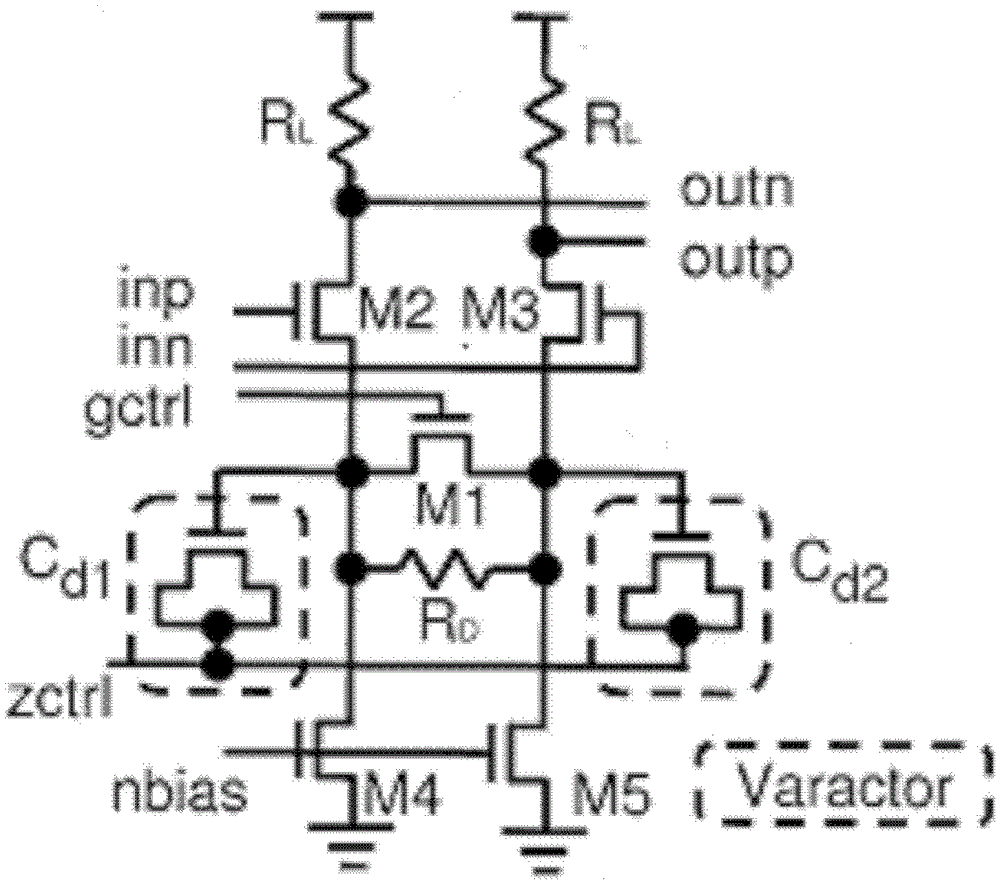
Figure 1 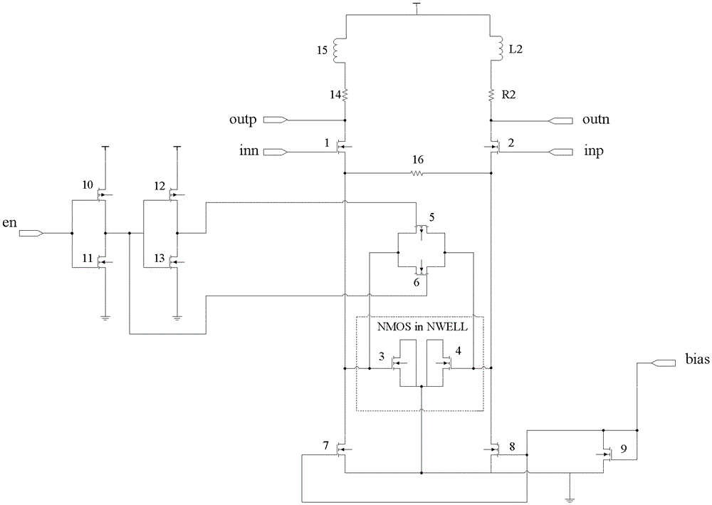
Figure 2 
Figure 3
Abstract
Description
technical field
[0001] The invention relates to a semiconductor integrated circuit, in particular to a linear equalizer. Background technique
[0002] The continuous improvement in the performance of CMOS integrated circuits has made it possible to transmit signals at speeds up to several Gb / s on cables or substrates. However, data serial communications at several Gb / s speeds are limited by bandwidth. Bandwidth limitation is mainly due to dielectric loss, skin effect and impedance discontinuity of the transmission medium. In a bandwidth-limited channel, when the data rate exceeds the bandwidth, the received signal will be severely distorted due to inter-symbol interference (ISI). In the prior art, an equalizer is usually used in a receiver to compensate or reduce ISI.
[0003] Choi et al. disclosed an equalizer in the article "A0.18-μmCMOS3.5-gb / scontinuous-timeadaptivecableequalizersingenhancedlow-frequencygaincontrolmethod". .419-425. Such as figure 1 Shown is a sche...
Examples
Embodiment Construction
[0023] Such as figure 2 Shown is a schematic structural diagram of a linear equalizer according to an embodiment of the present invention. The linear equalizer of the embodiment of the present invention includes:
[0024] A differential input pair is composed of a first MOS transistor 1 and a second MOS transistor 2, and both the first MOS transistor 1 and the second MOS transistor 2 are NMOS transistors. The gates of the first MOS transistor 1 and the second MOS transistor 2 are respectively input terminals of a pair of differential input signals inn and inp, and the drains of the first MOS transistor 1 and the second MOS transistor 2 are respectively a pair of The output terminals of the differential output signals outn and outp, the sources of the first MOS transistor 1 and the second MOS transistor 2 are respectively connected to a current source.
[0025] A first resistor 14 and a first inductor 15 are connected in series between the drain of the first MOS transistor 1...