
Signal Amplifier
a technology of signal amplifier and amplifier, which is applied in the direction of amplifier, amplifier with semiconductor devices/discharge tubes, amplifiers, etc., can solve the problems of lack of application flexibility and add zeros, and achieve the effect of increasing high frequency gain
Patent Information
- Authority / Receiving Office
- US · United States
- Patent Type
- Applications(United States)
- Current Assignee / Owner
- Publication Date
- 2014-01-30
- Estimated Expiration
- Not applicable · inactive patent
Smart Images
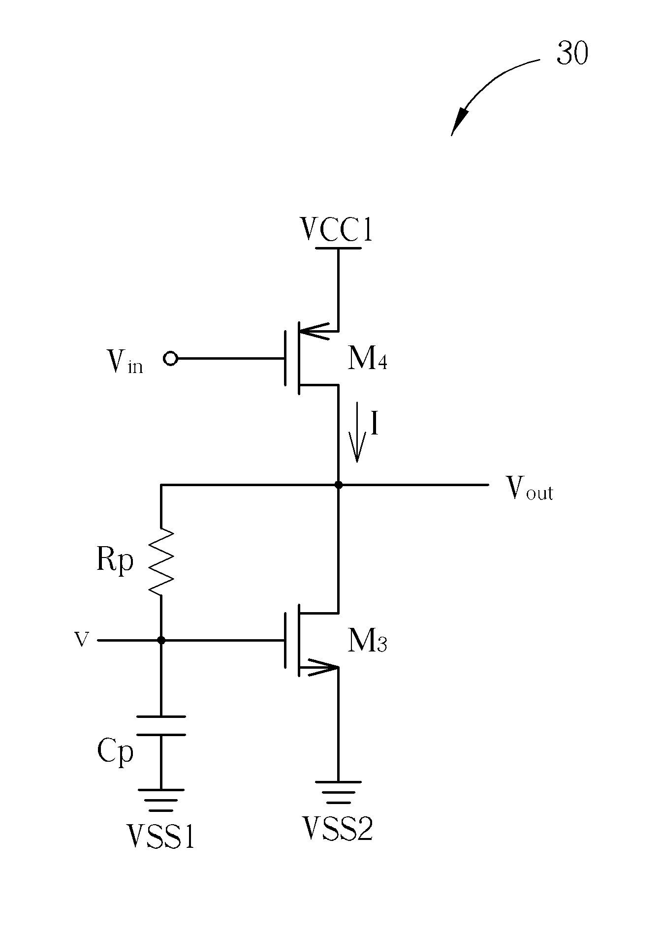
Figure 1 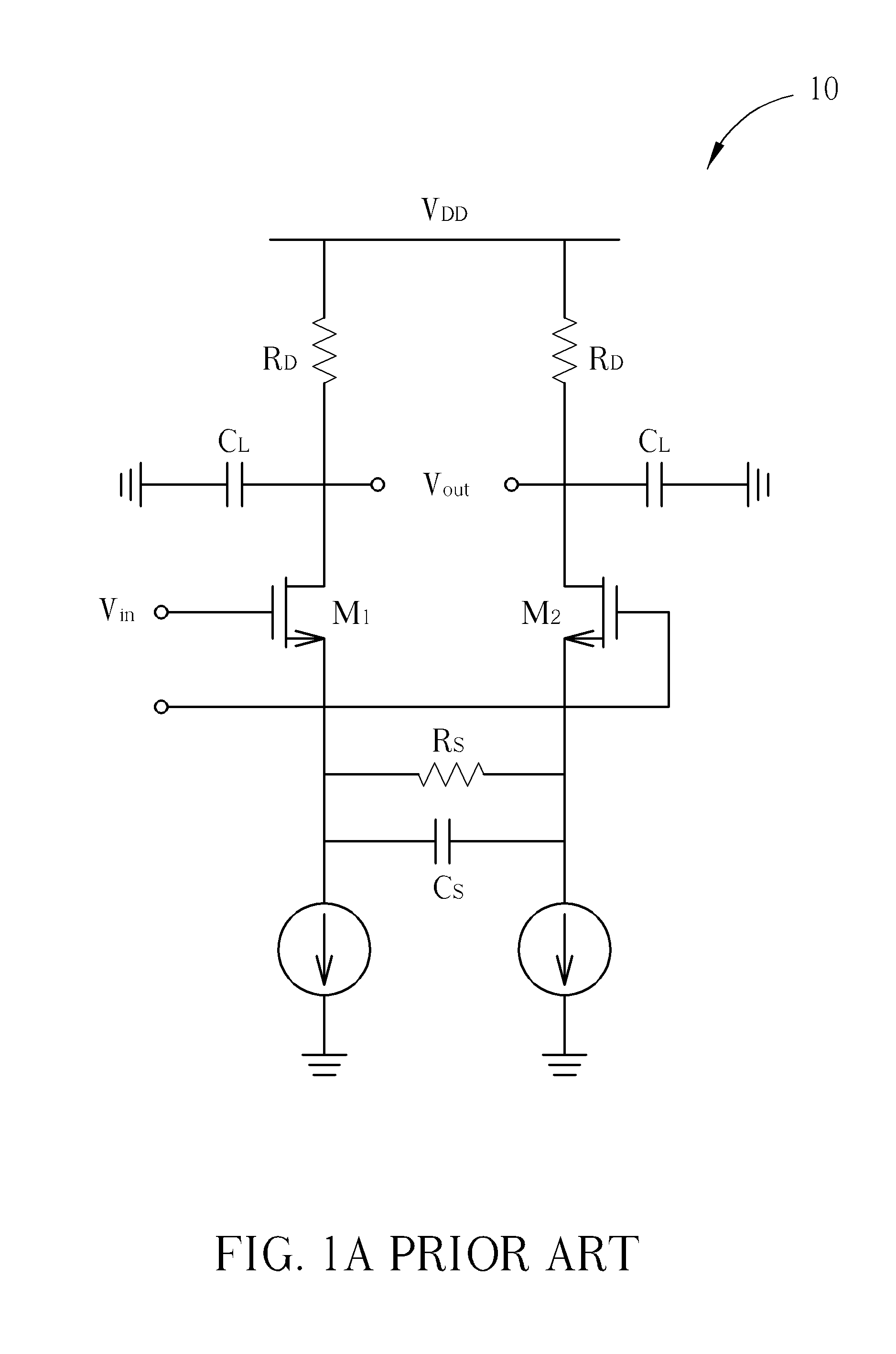
Figure 2 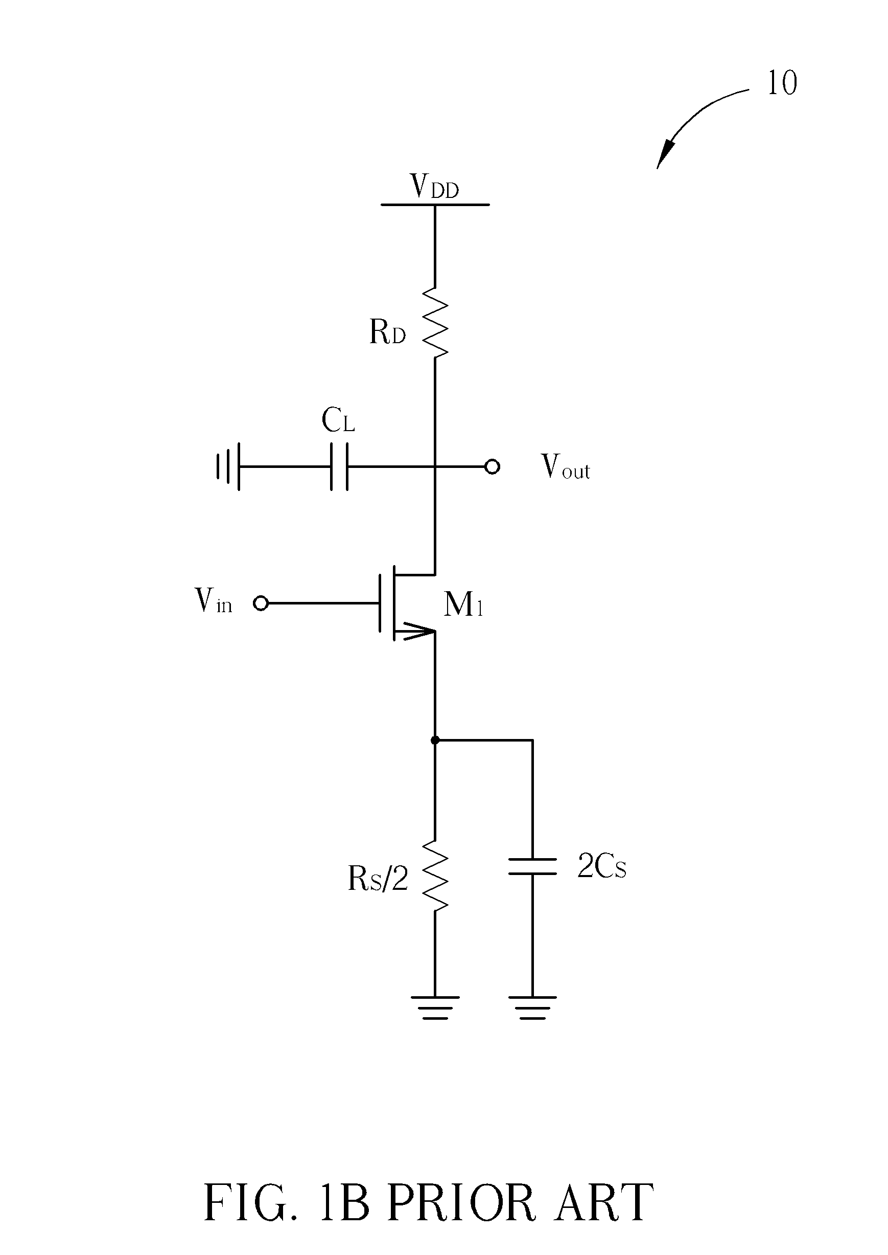
Figure 3
Abstract
Description
BACKGROUND OF THE INVENTION
[0001] 1. Field of the Invention
[0002] The present invention relates to a signal amplifier, and more particularly, to a signal amplifier capable of generating a zero for compensating signal attenuation to increase high frequency gain.
[0003] 2. Description of the Prior Art
[0004] In general, the signal amplifier has the phenomenon of signal attenuation due to the effect of low pass channel and the parasitic capacitance inside the amplifier. In order to compensate signal attenuation, the common method is to add a zero in the signal path to increase the signal gain for compensation. In the prior art, the common method of inserting a zero is using capacitive degeneration or inductive load, etc.
[0005] For example, please refer to FIG. 1A and FIG. 1B. FIG. 1A is a schematic diagram of a conventional differential signal amplifier 10 and FIG. 1B is a schematic diagram of small signal equivalent circuit of a part of the differential signal amplifier 10 in FIG. 1A. As sho...
Examples
Embodiment Construction
[0018]Please refer to FIG. 3A, which is a schematic diagram of a single-ended signal amplifier 30 according to an embodiment of the present invention. The single-ended signal amplifier 30 includes a transistor M3, a transistor M4, a resistor Rp, and a capacitor Cp. The detail structure and connection are as shown in FIG. 3. A terminal of the resistor Rp is coupled to a drain (i.e. a first terminal) of the transistor M3 and another terminal of the resistor Rp is coupled to a gate (i.e. a control terminal) of the transistor M3. A terminal of the capacitor Cp is coupled to the gate of the transistor M3 and another terminal of the capacitor Cp is coupled to a ground voltage VSS1 (i.e. a specific voltage). A drain of the transistor M4 is coupled to the drain of the transistor M3 and outputs an output voltage Vout, a gate of the transistor M4 is utilized for receiving an input voltage Vin, and a source (i.e. a second terminal) of the transistor M4 is coupled to a system voltage VCC1. A so...