
Semiconductor device
A semiconductor and transistor technology, applied in the field of semiconductor devices, can solve the problem of increasing the area of semiconductor devices, achieve the effect of reducing the area and suppressing the latch-up effect
Patent Information
- Authority / Receiving Office
- CN · China
- Patent Type
- Patents(China)
- Current Assignee / Owner
- Publication Date
- 2018-02-09
Smart Images
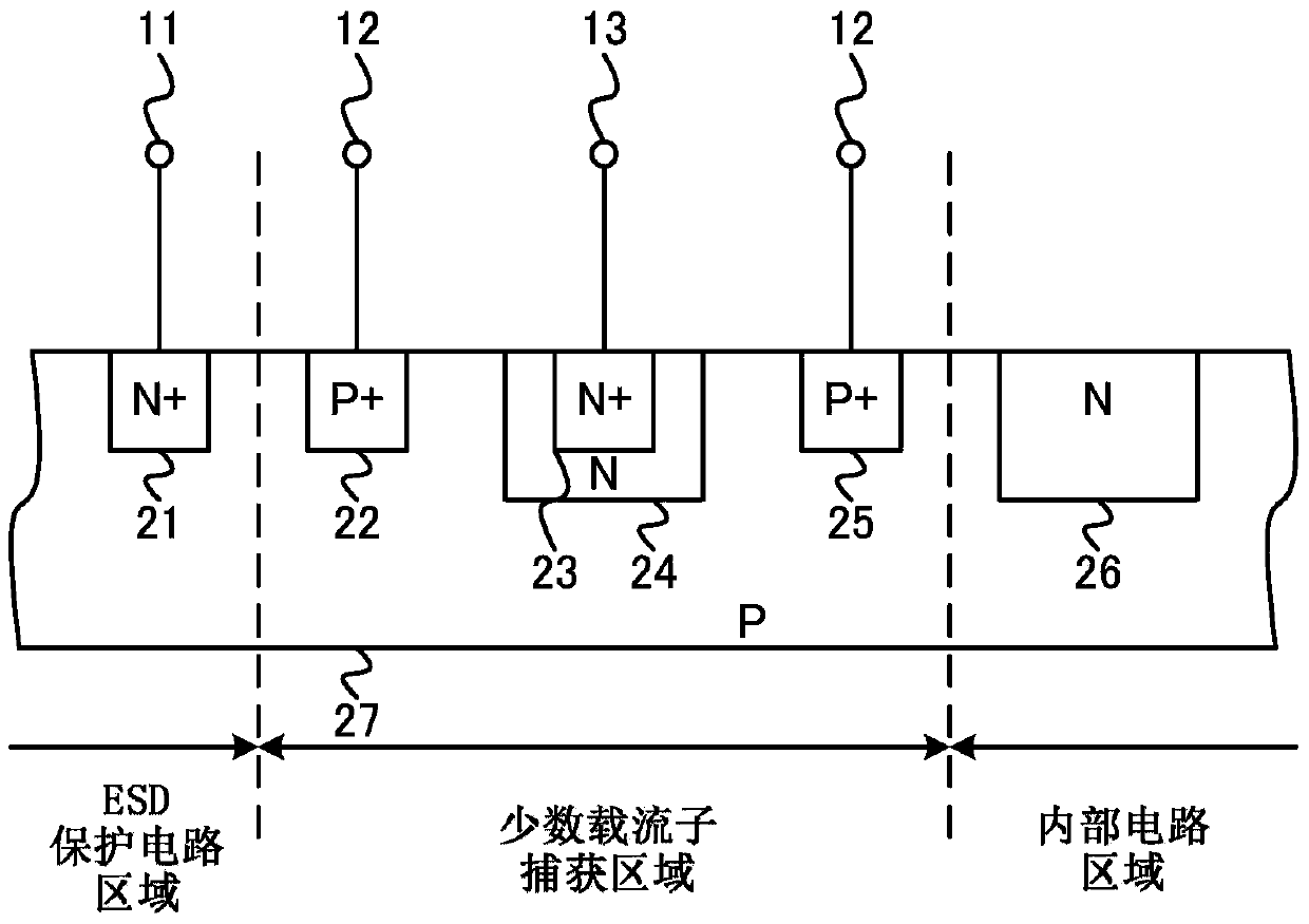
Figure 1 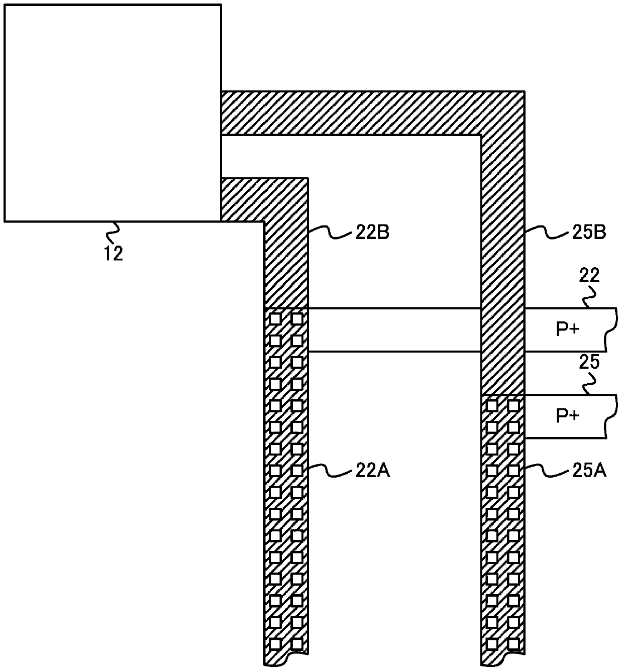
Figure 2 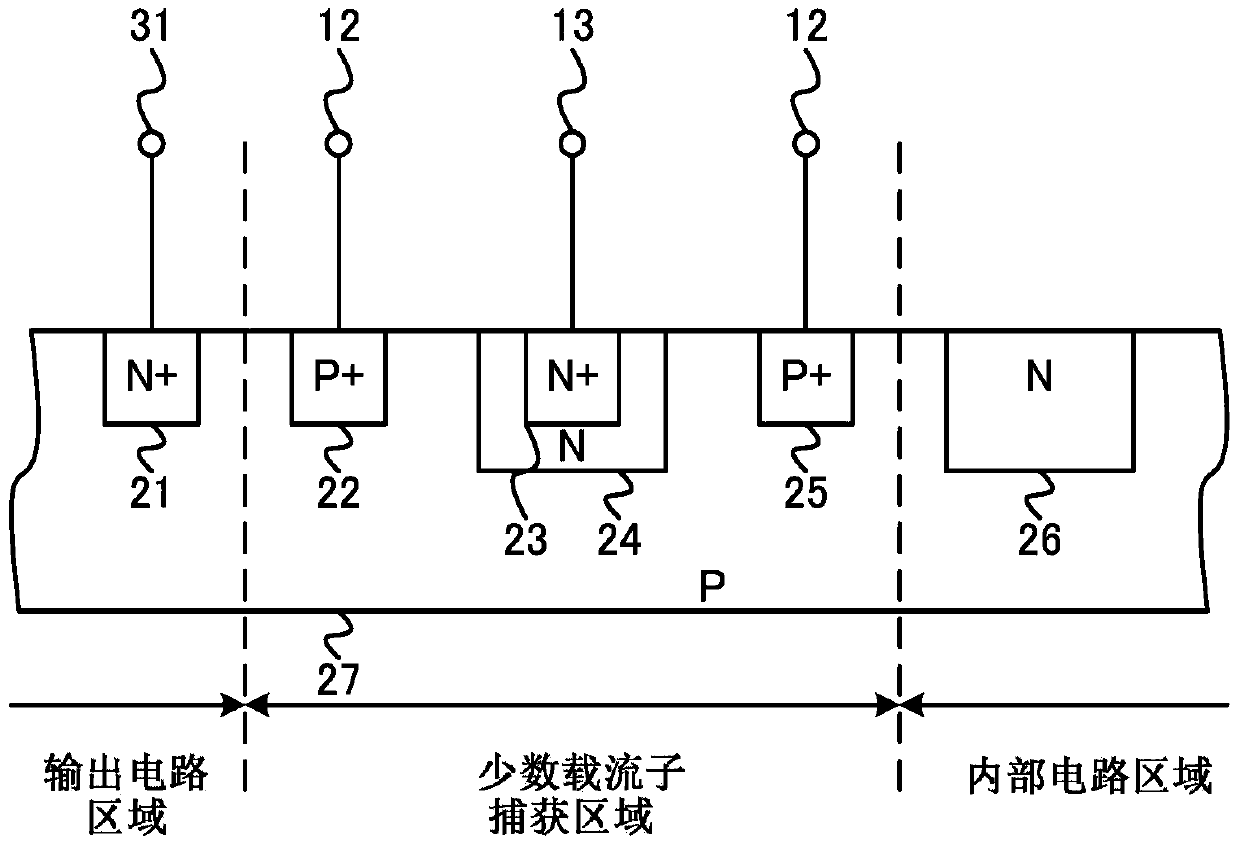
Figure 3
Abstract
Description
technical field
[0001] The present invention relates to semiconductor devices. More specifically, it relates to a semiconductor device capable of suppressing the occurrence of latch-up. Background technique
[0002] First, a conventional semiconductor device will be described. Figure 5 It is a sectional view showing a conventional semiconductor device.
[0003] When a surge with a negative voltage is applied to the input pad 71, electrons as minority carriers in the P-type semiconductor substrate 87 sometimes leak from the N-type diffusion region 81 in the ESD protection circuit region to the P-type semiconductor substrate 87 . The minority carriers flow from the semiconductor substrate 87 into the P-type diffusion region 82 connected to the ground pad 72 to be absorbed. Here, the length of the P-type diffusion region 82 in the horizontal direction in the direction from the ESD protection circuit toward the internal circuit is long enough so that minority carriers are su...
Examples
Embodiment Construction
[0025] Hereinafter, embodiments of the present invention will be described with reference to the drawings. First, the structure of the semiconductor device will be described. figure 1 is a cross-sectional view showing a semiconductor device, figure 2 It is a top view showing a semiconductor device.
[0026] Such as figure 1 As shown, the semiconductor substrate 27 is composed of three regions, the ESD protection circuit region, the internal circuit region and the minority carrier trapping region. The ESD protection circuit region is used to protect the semiconductor device from the influence of ESD, and the minority carrier The carrier trapping region traps minority carriers generated in the semiconductor substrate 27 due to a surge having a negative voltage applied to the pad 11 of the input or output, the minority carrier trapping region surrounds the internal circuit area, usually forming a protective ring. The input or output pad 11, the ground pad 12, the power pad...