
A slot-gate short-circuited anode soi LIGBT
A trench gate, anode technology, applied in circuits, semiconductor devices, electrical components, etc., can solve the problems of large on-voltage drop, low anode hole injection efficiency, affecting the uniformity of device current distribution, etc., to reduce the on-voltage drop, eliminate the phenomenon of voltage foldback, eliminate the effect of voltage foldback effect
Patent Information
- Authority / Receiving Office
- CN · China
- Patent Type
- Patents(China)
- Current Assignee / Owner
- Publication Date
- 2020-05-26
Smart Images
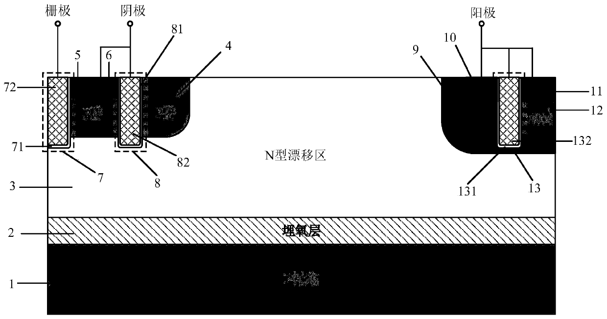
Figure 1 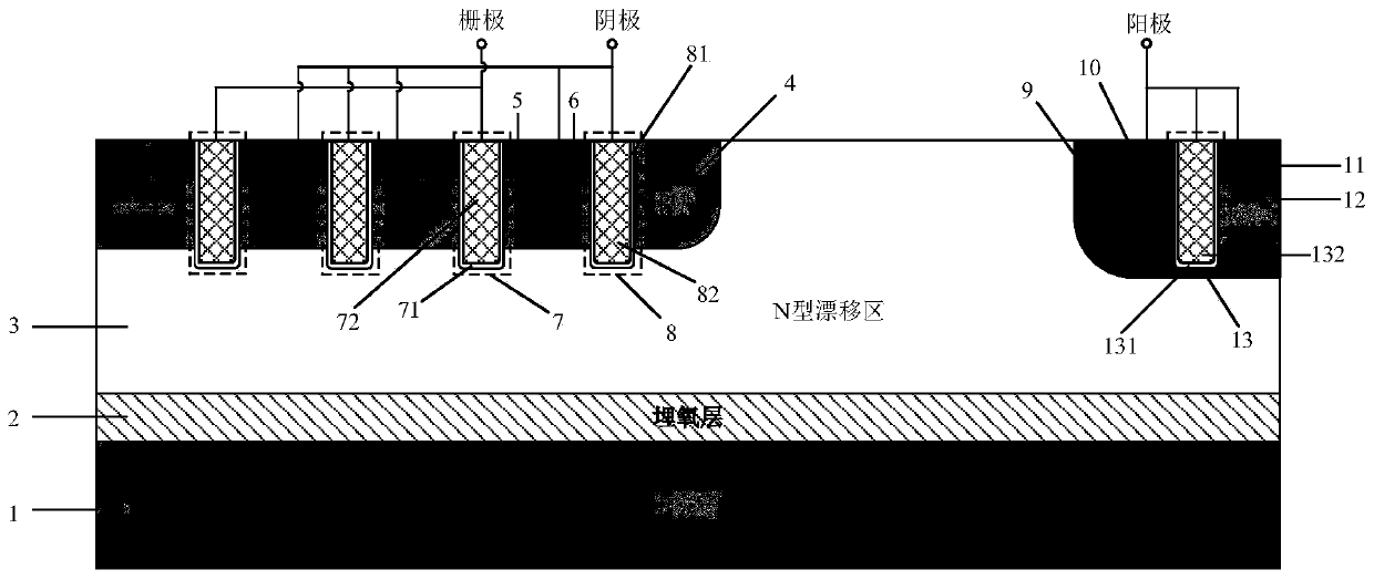
Figure 2 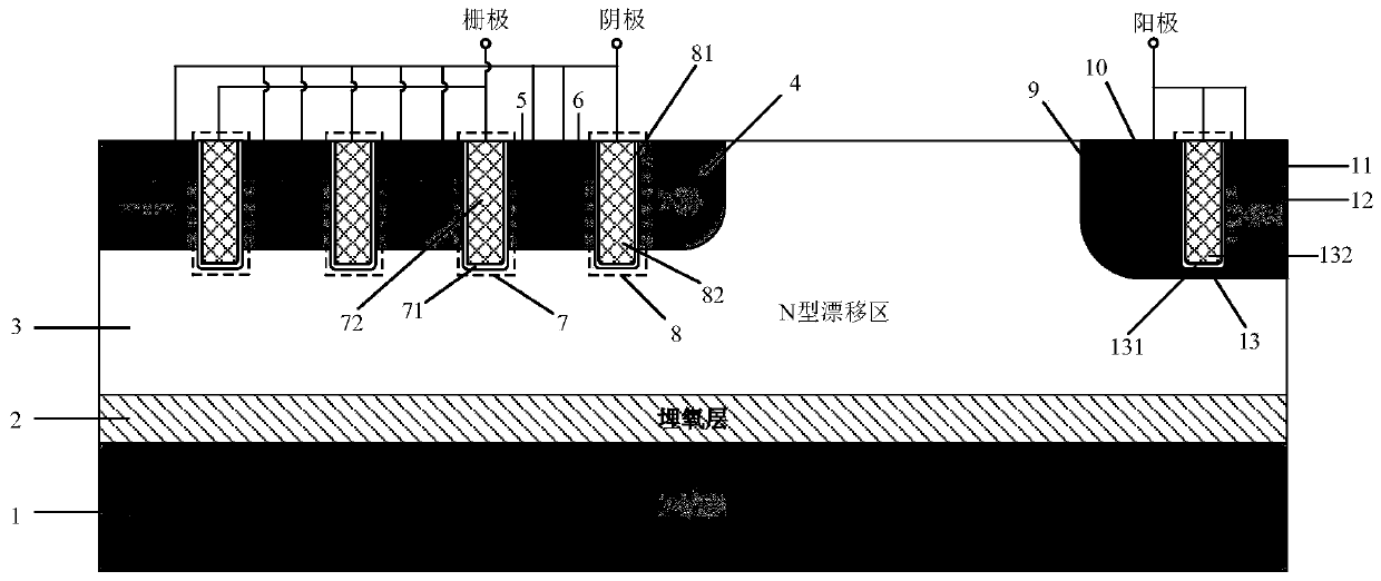
Figure 3
Abstract
Description
technical field
[0001] The invention belongs to the technical field of power semiconductors, and relates to a slot-gate short-circuited anode SOI LIGBT (Lateral Insulated Gate Bipolar Transistor, lateral insulated gate bipolar transistor). Background technique
[0002] IGBT is a new device combining MOSFET (Metal Oxide Semiconductor Field Effect Transistor) and BJT (Bipolar Junction Transistor). It not only has the advantages of high input impedance of MOSFET and low on-resistance of BJT, but also realizes High breakdown voltage and high forward current. Among them, lateral IGBT (LIGBT) is easy to be integrated in silicon-based, especially SOI-based power integrated circuits. SOI-based LIGBT can completely eliminate the hole-electron injection of bulk silicon LIGBT substrate, and the use of dielectric isolation SOI technology is easy to achieve device integration. Complete electrical isolation makes SOI LIGBT widely used in high-tech industries such as power electronics, in...
Examples
Embodiment 1
[0019] like figure 1 As shown, the SOI LIGBT of this example includes a P substrate 1, a buried oxide layer 2, and a top semiconductor layer stacked sequentially from bottom to top; the top semiconductor layer has an N-type drift region 3, and an N-type drift region 3 One side has a P well region 4, and the other side is an anode structure; the upper surface of the P well region 4 has an N+ cathode region 5 and a P+ body contact region 6, and the lead end of the P+ body contact region 6 is a cathode; In the well region 4, there are groove grids 7 and cathode grooves 8 that penetrate the P well region 4 from the surface and extend from the bottom to the N-type semiconductor drift region 3, and the groove grids 7 are in contact with the N+ cathode region 5, and the cathode grooves 8 In contact with the P+ body contact region 6, the slot grid 7 and the cathode slot 8 respectively have a first insulating dielectric layer 71 and a second insulating dielectric layer 81 located on th...
Embodiment 2
[0023] like figure 2 As shown, compared with Embodiment 1, there are multiple slot gates 7 and cathode slots 8 in this example, which are alternately arranged along the lateral direction of the device. Multiple trench gates increase the channel density of the device and reduce the conduction voltage drop.
Embodiment 3
[0025] like image 3 As shown, compared with Embodiment 2, the N+ cathode region 5 is connected to the cathode in this example.