
Real-time feedback automatic assembling and manufacturing method for nano-electronic appliance
A real-time feedback, electronic device technology, applied in nanostructure manufacturing, semiconductor/solid-state device manufacturing, nanostructure assembly, etc. Effect
Patent Information
- Authority / Receiving Office
- CN · China
- Patent Type
- Applications(China)
- Current Assignee / Owner
- Publication Date
- 2015-02-18
- Estimated Expiration
- Not applicable · inactive patent
Smart Images
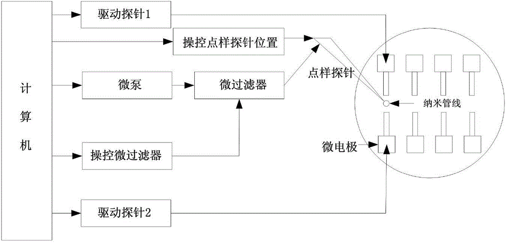
Figure 1 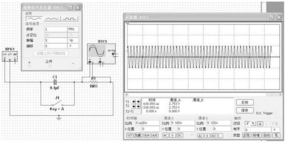
Figure 2 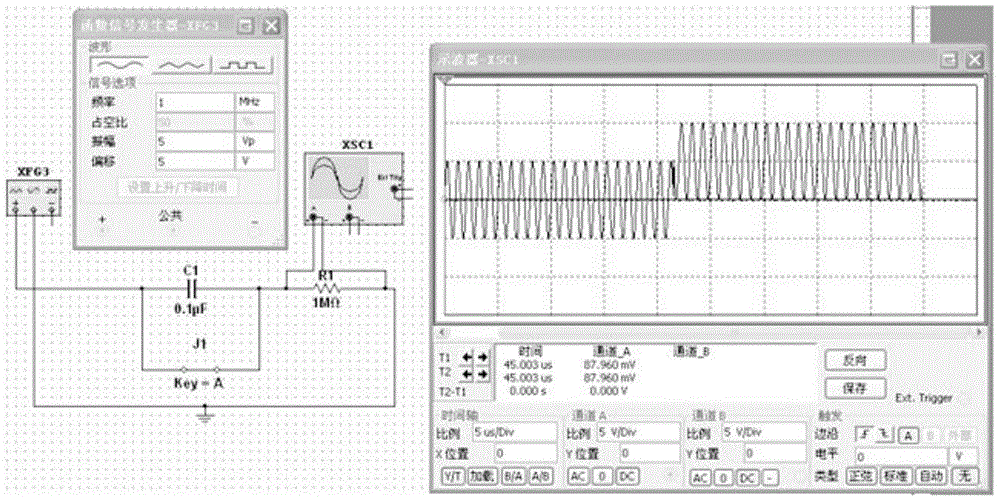
Figure 3
Abstract
Description
technical field
[0001] The invention relates to the field of nanometer operation, in particular to an automatic assembly and manufacturing method of nanometer electronic devices with real-time feedback. Background technique
[0002] Nanotechnology and nanodevices are one of the important development directions of today's high-tech. The breakthrough of nanotechnology and the application of nanodevices depend on the progress of nanofabrication technology. According to the December 2007 technical report (ITRS2007) of the International Technology Roadmap for Semiconductors (ITRS), by 2020, the half-pitch width of DRAM will be 14nm. With the continuous reduction of device size, it will be getting closer and closer to the limit of the existing electronic component architecture. The insurmountable problems encountered are not only the physical limit of electronic devices, but also precision automatic processing and power consumption. technical bottleneck. The traditional silicon...
Examples
Embodiment Construction
[0019] The present invention will be described in further detail below in conjunction with the accompanying drawings.
[0020] 1. Pretreatment of nanomaterials: put ZnO nanowires and alcohol mixed solution at a ratio of 1:1000 into a test tube, put the test tube into an ultrasonic oscillator at 30 degrees Celsius for 10-15 minutes, then take it out and stand still for 1 hour to obtain a uniform Translucent solution, obtain a large number of ZnO nanowire samples dispersed in the solution as a single;
[0021] 2. Automatic assembly process based on a closed-loop control system: Since the distance between the source and drain electrodes is about 1 μm, it is equivalent to a capacitor in the circuit. When the ZnO nanowire is not overlapped, the AC signal can be transmitted through the electrode, and the DC signal will be blocked. ; When the medium is lapped at both ends of the electrode, the electrode and the medium are equivalent to a resistance, and both AC and DC signals can be ...