
A kind of semiconductor element and its preparation method
A semiconductor and component technology, applied in the field of semiconductor components and their preparation, can solve problems such as inconsistency in the ability to release stress, damage to the performance of semiconductor devices, and poor compactness of the aluminum nitride layer, so as to avoid cracks and pores and reduce device leakage phenomenon, the effect of reducing lattice differences
Patent Information
- Authority / Receiving Office
- CN · China
- Patent Type
- Patents(China)
- Current Assignee / Owner
- Publication Date
- 2018-07-10
Smart Images
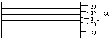
Figure 1 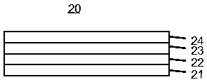
Figure 2 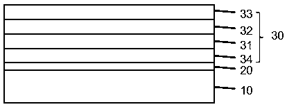
Figure 3
Abstract
Description
technical field
[0001] The invention belongs to the technical field of semiconductors, in particular to a semiconductor element and a preparation method thereof. Background technique
[0002] The physical vapor deposition method (PVD method) has the characteristics of simple process, less environmental pollution, less raw material consumption, uniform and dense film formation, and strong bonding with the substrate. It is currently being increasingly used in the preparation of semiconductor components. Among them, it is usually used for the preparation of the bottom layer, such as depositing an aluminum nitride layer as a buffer layer, which can reduce and buffer defects and stresses caused by lattice mismatch and thermal mismatch between the substrate and the epitaxial layer, and improve semiconductor performance. Component quality.
[0003] Compared with chemical vapor deposition, the atoms sputtered by PVD method have higher energy (generally 10~20eV) and stronger migrati...
Examples
Embodiment 1
[0034] See attached Figure 1~2 , the present embodiment provides a semiconductor element, which includes: a silicon substrate 10, a multi-layer buffer structure 20 and an epitaxial functional layer 30, where the epitaxial functional layer 30 is a first semiconductor layer 31, a light emitting layer 32 and a second The light-emitting diode epitaxial layer composed of two semiconductor layers 33; the first semiconductor layer 31 and the second semiconductor layer 33 are respectively a semiconductor layer doped with donor impurities and a semiconductor layer doped with acceptor impurities. Of course, the non-doped semiconductor layer 34 can also be included in the semiconductor element of the present invention (see the attached image 3 ). The multi-layer buffer structure 20 consists of an aluminum metal protective layer 21 with a thickness of 1-100 angstroms, an aluminum oxide metal oxide protective layer 22 with a thickness of 1-500 angstroms, and an oxygen-doped aluminum nit...
Embodiment 2
[0044] See attached Figure 4 The difference between this embodiment and Embodiment 1 is that a transistor epitaxial layer is deposited on the surface of the multilayer buffer structure 20 as an epitaxial functional layer 30 to form a transistor element. The preparation method and structure are as follows: the aluminum metal protection layer 21, the oxide The substrate of the multilayer buffer structure 20 composed of the aluminum metal oxide protection layer 22, the oxygen-doped aluminum nitride transition layer 23 and the oxygen-doped aluminum nitride buffer layer 24 is transferred into the MOCVD chamber, and aluminum gallium nitride is deposited by the MOCVD method layer 35 to further buffer the lattice stress of the multilayer buffer structure 20 to avoid cracks; then another layer 36 of gallium nitride semiconductor layer 36 that is not intentionally doped or doped with carbon or doped with iron, and then deposited aluminum gallium nitride semiconductor Layer 37, the AlGa...