
A device and method for measuring film strain and thermal conductivity
A technology of thermal conductivity and thin film, applied in the field of MEMS device devices of micro-electromechanical systems, can solve the problems of complex, unequal, and unsatisfactory devices, and achieve the effects of easy operation, simple structure, mature and reliable
Patent Information
- Authority / Receiving Office
- CN · China
- Patent Type
- Patents(China)
- Current Assignee / Owner
- Publication Date
- 2019-04-12
Smart Images
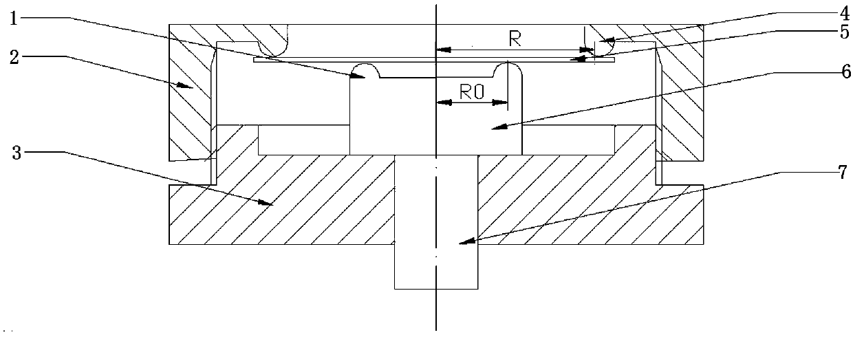
Figure 1 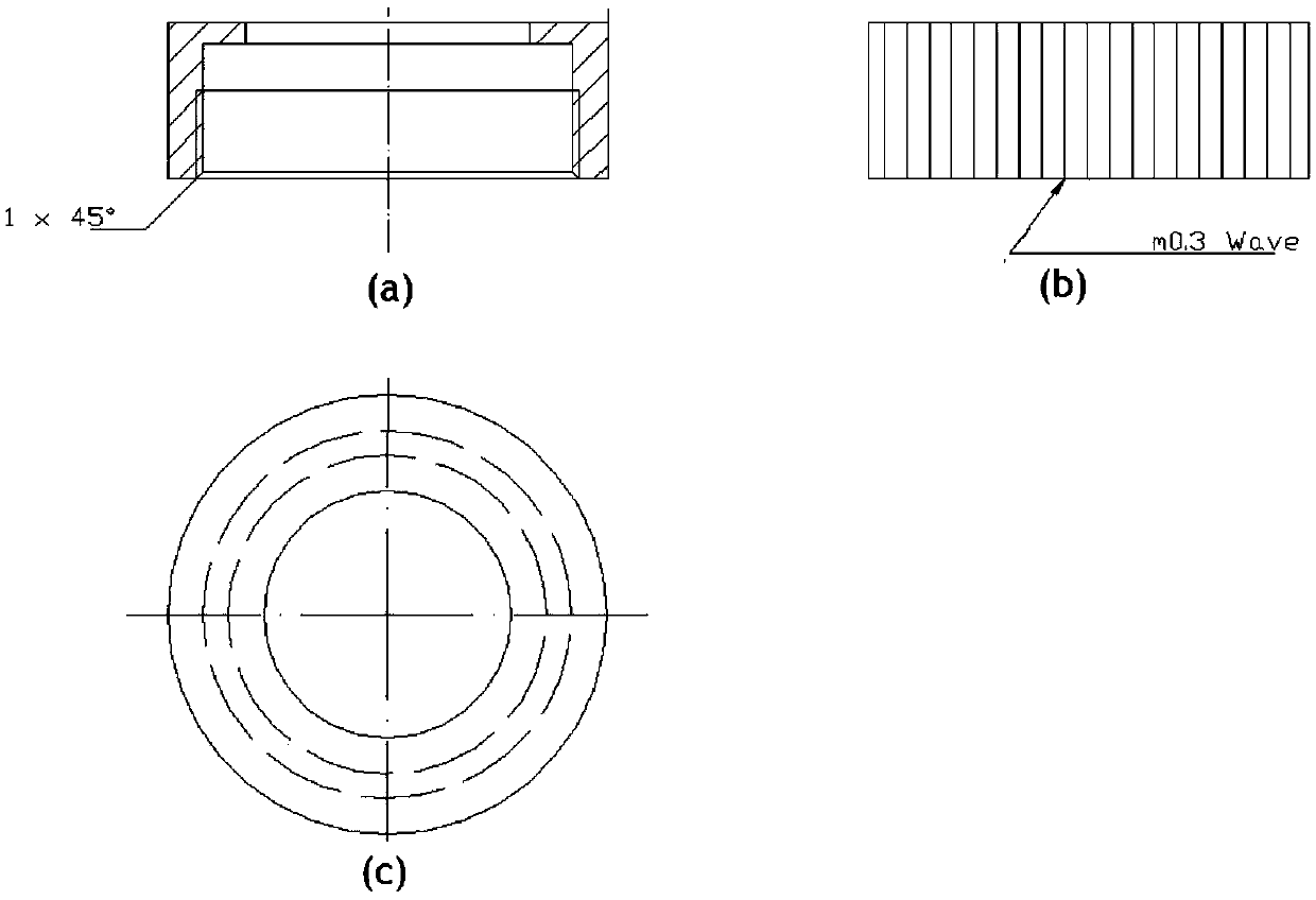
Figure 2 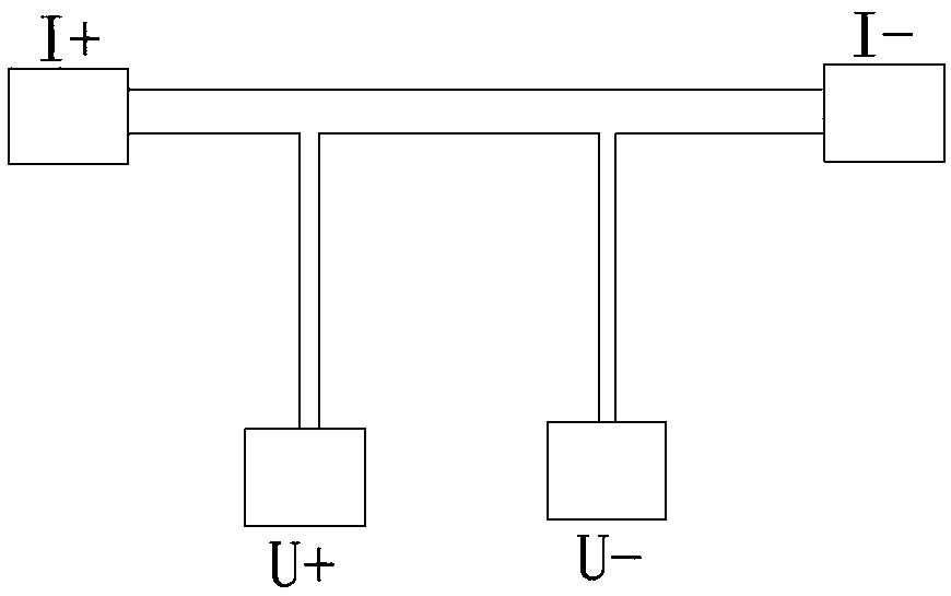
Figure 3
Abstract
Description
technical field
[0001] The invention relates to a MEMS device device of a micro-electromechanical system, in particular to a device and a method for measuring film strain and thermal conductivity. Background technique
[0002] With the rapid development of micro-electromechanical system MEMS technology, various thin-film devices with excellent performance have emerged. Among them, there are more and more types of MEMS devices that work under thermal fields, and the amount of them is also increasing, such as micro-infrared light sources, Micro-gas sensors and high-temperature MEMS pressure sensors have operating temperatures of hundreds or even thousands of degrees Celsius, and there are alternating temperature fields, which put forward higher requirements for the reliability of thin-film structures and materials in service. Especially in the field of sensors, when measuring some basic physical quantities, the device will inevitably undergo corresponding deformation and strai...
Examples
Embodiment Construction
[0030] The invention will be further described in detail below in conjunction with the accompanying drawings and embodiments, but it is not used as a basis for any limitation on the invention.
[0031] Such as figure 1 , figure 2 Shown in (a)-(c), the device for measuring thin film strain and thermal conductivity of the present invention includes a base 3, a shell 2 arranged on the base 3, the base 3 is provided with a loading end 6, coated with a thin film The substrate 5 is placed on the loading end 6 and connected to the simply supported fixed end 4 on the upper part of the housing 2, a precision guide rod 7 is provided under the loading end 6, and a test electrode and a metal plate are sputtered on the substrate 5 coated with a thin film. The test electrode is connected to the detection system with an external lock-in amplifier module and connected to the computer; the precession displacement S of the precision guide rod 7 makes the film on the substrate 5 coated with th...