
Process for preparing high-C-axis-orientation ScAlN thin film
A film and orientation technology, which is applied in the process of preparing highly C-axis oriented ScAlN films, can solve the problems of reducing the selection range of substrate materials, high-power vacuum space, unfavorable industrial production, etc., and achieves the elimination of heating and cooling bases. The effect of slice time, energy saving, time reduction
Patent Information
- Authority / Receiving Office
- CN · China
- Patent Type
- Applications(China)
- Current Assignee / Owner
- Publication Date
- 2017-07-04
- Estimated Expiration
- Not applicable · inactive patent
Smart Images
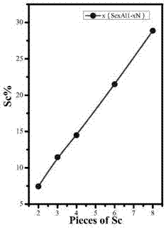
Figure 1 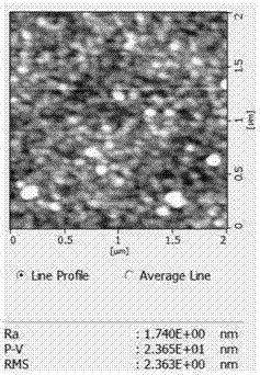
Figure 2 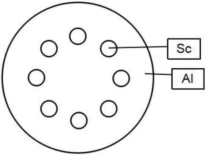
Figure 3
Abstract
Description
technical field
[0001] The invention relates to a preparation process for preparing a ScAlN film, that is, a process for preparing a ScAlN film with high C-axis orientation by radio frequency magnetron sputtering and its optimization. Background technique
[0002] The magnetic field sensor developed by magnetoelectric composite materials has high sensitivity and small volume, adapts to the trend of miniaturized devices, and can be used in many fields such as geophysics, national defense and military, and biomedicine. A variety of sensor structures combined with magnetoelectric composite materials, surface acoustic wave technology or bulk acoustic wave technology proposed in recent years can enable the sensor to be applied to both DC and broadband AC magnetic field detection while achieving high sensitivity, which meets the application requirements. In order to obtain a magnetic field sensor with better performance. The piezoelectric film in this structure has become a resea...
Examples
Embodiment 1
[0030] The processing steps in the present embodiment are as follows:
[0031] Step 1: Using Si(100) as the substrate, first soak the substrate in a mixed liquid of concentrated sulfuric acid and hydrogen peroxide (liquid volume ratio H 2 SO 4 :H 2 o 2 =1:1) for 30 minutes to remove stubborn stains on the surface, then ultrasonically clean the substrate in acetone for 20 minutes, ultrasonically clean in alcohol for 10 minutes to remove surface organic pollutants, and finally use high-purity argon to dry it and place it in a sputter The ejaculation room is spare.
[0032] Step 2: Polish the surface of the Al target (99.999%) with a diameter of Φ=75mm and the Sc target (99.999%) with a diameter of Φ8mm until the surface is bright with 1000-mesh sandpaper, clean the surface stains with alcohol, and dry them with high-purity nitrogen. The sputtering track of the target is divided into four areas equally. One side of the 4 pieces of Sc target is coated with silver paste and pas...
Embodiment 2
[0040] The processing steps in the present embodiment are as follows:
[0041] Step 1: Si (100) is used as the substrate, and the processing method of the substrate is the same as that in the first embodiment.
[0042] Target processing:
[0043] Step 2: Al target (99.999%) and Sc target (99.999%) chip targets are used as sputtering targets, and chip target materials are implemented in the same way as in Example 1.
[0044] Step 3: Treat the Si(100) substrate in the same way as in Step 1 and grow a layer of Si on the surface of the substrate 3 N 4 layer, put the processed substrate into the PECVD instrument, and Table 2 sets the process parameters.
[0045] Table 2 Partial experimental conditions of SiN prepared by PECVD
[0046] Power / W Pressure / mT Si / Ar / sccm N2 / sccm Time / s 60 400 250 200 100
[0047] Step 4: Put the target processed in step 2 and the Si3N4 / Si substrate prepared in step 3 into the vacuum chamber. The pre-sputtering condition...