
Phase change thin film structure, phase change memory unit, manufacturing method thereof and phase change memory
A technology of phase-change memory and thin-film structure, which is applied in the field of phase-change memory, can solve problems such as poor reliability, reduced tolerance to noise resistance, and changes in resistance value, and achieve the effects of controllable growth process and adjustable crystallization temperature
Patent Information
- Authority / Receiving Office
- CN · China
- Current Assignee / Owner
- Publication Date
- 2019-06-25
Smart Images
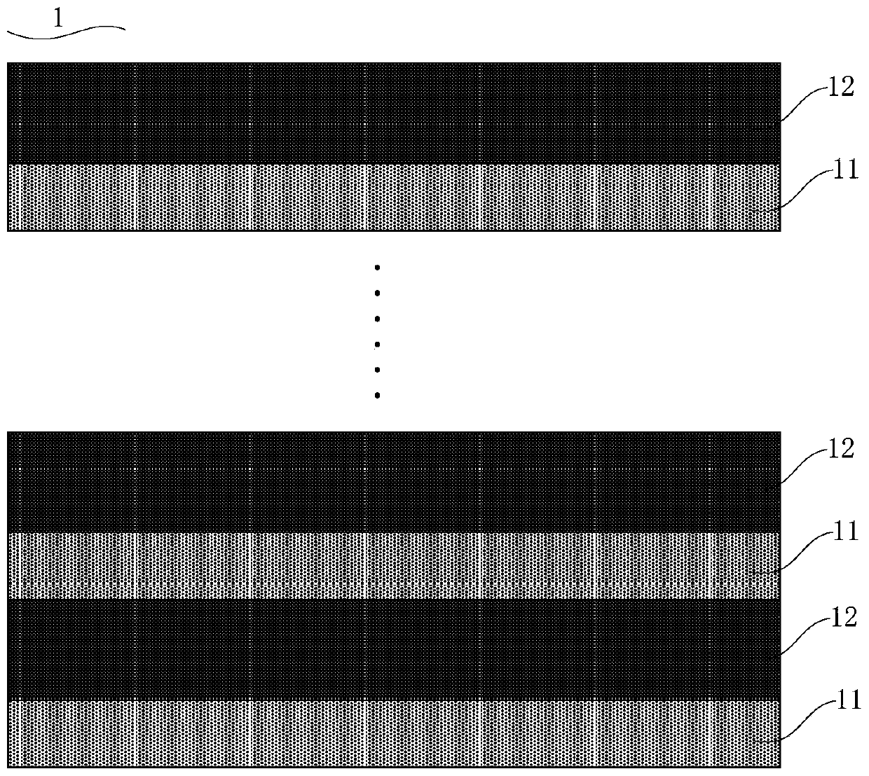
Figure 1 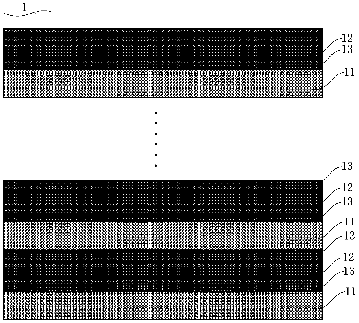
Figure 2 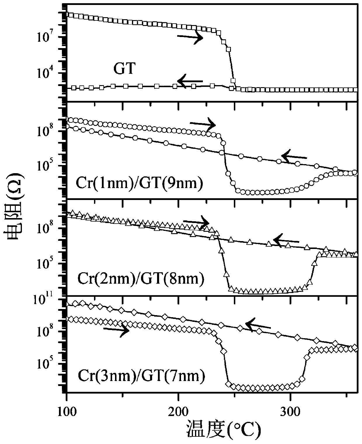
Figure 3
Abstract
Description
technical field
[0001] The invention belongs to the technical field of phase-change memory, and in particular relates to a phase-change film structure, a phase-change memory unit, a preparation method thereof, and a phase-change memory. Background technique
[0002] The method adopted by the traditional multi-state storage technology is to obtain resistance states with different resistance values by applying different numbers of programming pulses to the PCRAM (Phase Change Random Access Memory) in the RESET state. The basic principle is that the grain growth of the phase change material is a continuous and gradual process, and the number of programming pulses can control the crystallization ratio of the phase change material in the PCRAM. However, multi-valued storage based on different crystallization ratios has obvious shortcomings. Only the high-resistance state and the low-resistance state are two stable states, which appear as two gentle "steps" between the high-resi...
Examples
Embodiment 1
[0052] Such as figure 1 As shown, the present invention provides a phase change thin film structure 1, and the phase change thin film structure 1 comprises:
[0053] Cr layer 11;
[0054] Ge x Te 100-x layer 12, where x is the Ge x Te 100-x Atomic percentage of Ge in layer 12, 0
[0055] The Cr layer 11 and the Ge x Te 100-x Layers 12 are alternately stacked one after the other.
[0056] As an example, one layer of the Cr layer 11 in the phase-change thin film structure 1 and the adjacent layer of Ge x Te 100-x Layer 12 is called an alternately stacked cycle, and the Cr layer 11 and the Ge layer in the phase change film structure 1 x Te 100-x The number of periods in which the layers 12 are alternately stacked can be set according to actual needs, for example, the Cr layer 11 and the Ge layer in the phase change film structure 1 x Te 100-x The number of periods in which layers 12 are stacked alternately may include but not limited to 1-30.
[0057] As an e...
example 1
[0071]In this example, the Ge in the phase change thin film structure 1 x Te 100-x In layer 12, x=40, the thickness of the Cr layer 11 is 1nm, the Ge x Te 100-x The thickness of layer 12 is 9nm, and the Cr layer 11 and the Ge in the phase change film structure 1 x Te 100-x The number of periods in which layers 12 are stacked alternately is 5. At this time, the expression of the phase-change film structure 1 can be expressed as [Cr(1nm) / Ge 40 Te 60 (9nm)] 5 .
[0072] The specific preparation method of the phase-change thin film structure 1 in this example includes the following steps:
[0073] 1) Substrate (the substrate) preparation.
[0074] Select a SiO2 / Si(100) substrate with a size of 5mm*5mm, first ultrasonically clean the substrate in acetone (a purity of 99% or more) in an ultrasonic cleaner for 3 to 5 minutes, and take it out with a deionized Rinse with water; then in an ultrasonic cleaning machine, the substrate is ultrasonically cleaned in ethanol (purity a...
example 2
[0084] The expression of phase-change thin film structure 1 described in this example can be [Cr (2nm) / Ge 40 Te 60 (8nm)] 5 The rest of the preparation method are the same as example 1, the difference is: step 3) magnetron sputtering prepares [Cr(2nm) / Ge 40 Te 60 (8nm)] 5 During multi-layer composite film, the sputtering time of each layer of Cr layer 11 is 6s, each layer of Ge 40 Te 60 The sputtering time of the film was 20s.