
High-resolution spatial omics detection method for tissue sample
A tissue sample and spatial omics technology, which is applied in the field of high-resolution spatial omics detection of tissue samples, can solve the difference of oligonucleotide sequence region modification effect, increase product cost and design complexity, and cross tissue spatial sequence information. Pollution and other problems, to achieve the effect of reducing material costs, reducing instrument costs, and reducing the types of use
Patent Information
- Authority / Receiving Office
- CN · China
- Patent Type
- Applications(China)
- Current Assignee / Owner
- Publication Date
- 2021-11-05
Smart Images
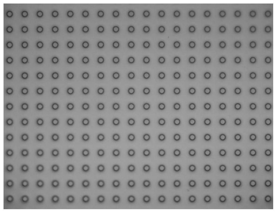
Figure 1 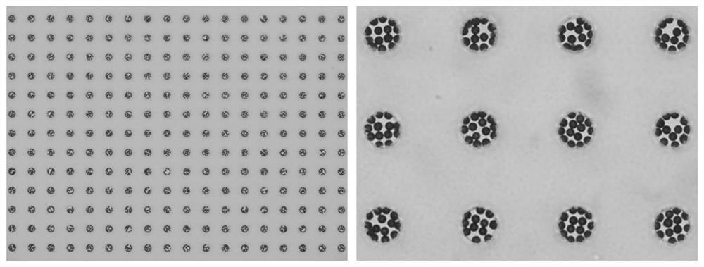
Figure 2 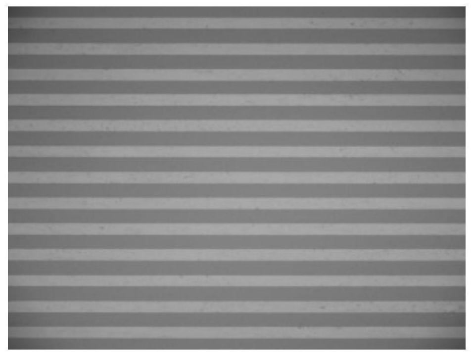
Figure 3
Abstract
Description
technical field
[0001] The present invention mainly relates to a high-resolution spatial omics detection device, system and method for tissue samples, in particular to a high-resolution spatial omics detection method for tissue samples. Background technique
[0002] Human tissue is a highly complex system composed of trillions of cells, which vary in type, time and space. For example, tissues in different regions of the mammalian brain have different functions and cell types. Qualitative testing is particularly important. Spatial omics refers to the omics research that is done on tissue slices and retains the spatial information of the sample. Spatial omics can display the gene expression in different regions of tissue slices, reveal the activated signaling pathways in fine pathological regions, and complete the mechanism analysis of molecular features driving pathological features. Space omics has completed the technical innovation of pathological digitalization combined ...
Examples
Embodiment 1
[0138] Embodiment 1: Microwell slide preparation
[0139] Expose the glass plate with a uniform chromium film and photoresist layer under the mask plate of the transparent array for 10s, and then soak the substrate in the developer solution for 30s to obtain a patterned photoresist with a chromium layer. Resist the surface of the array glass slide; then place it in a chromium etching solution and soak it for 5 minutes, then place the glass slide in a glass etching solution (mass ratio HF:HNO 3 : NH 4 F: H 2 (0=25:23.5:9.35:450) soaked in 80min to obtain the patterned microwell array glass slide ( figure 1 ), where the height of the microwells is 40 μm, the diameter is 30 μm, and the distance between the centers of the microwells is 60 μm.
Embodiment 2
[0140] Embodiment 2: preparation of micro reaction chamber
[0141] Spread the microbead carrier suspension with a diameter of 5-7 μm on the surface of the microwell slide, let it stand for 5 minutes, the microbeads settle in the microwell array, wash the surface of the microwell slide, and wash away the microbeads outside the microwell array, A microwell reaction chamber array containing microbeads was obtained ( figure 2 ).
Embodiment 3
[0142] Embodiment 3: the preparation of microchip
[0143] Place the glass plate with a uniform chrome film and photoresist layer under a mask with parallel holes and expose it to a UV lamp for 10s, then soak the substrate in a developer solution for 30s to obtain micropores with a chromium layer patterned photoresist glass surface; then place it in chrome etching solution for 5 minutes, then place the surface in glass etching solution (mass ratio HF:HNO 3 : NH 4 F: H 2 O=25:23.5:9.35:450) soaked in 40min to obtain the glass channel mold of the morphology structure of the microchannel pattern; polydimethylsiloxane (PDMS) prepolymer and curing agent are in mass ratio of 10:1 Mix the ratio evenly, and after vacuum degassing for 30 minutes, pour it onto the surface of the glass mold, place it in an oven with a temperature of 60°C, cure it for 10 hours, and lift it off to obtain PDMS microfluidic channels arranged in parallel ( image 3 ), the channel height is 20 μm, the width...