
Read voltage optimization method, memory storage device and memory control circuit unit
a technology of read voltage and optimization method, which is applied in the direction of digital storage, static storage, instruments, etc., can solve the problems of large amount of computing resources, limited number of adjustment read voltage sets, and resource-consuming conventional processes for adjusting read voltage sets to obtain optimal read voltage sets. achieve the effect of quick and efficient optimization of read voltage sets
Patent Information
- Authority / Receiving Office
- US · United States
- Patent Type
- Patents(United States)
- Current Assignee / Owner
- Publication Date
- 2019-11-19
Smart Images
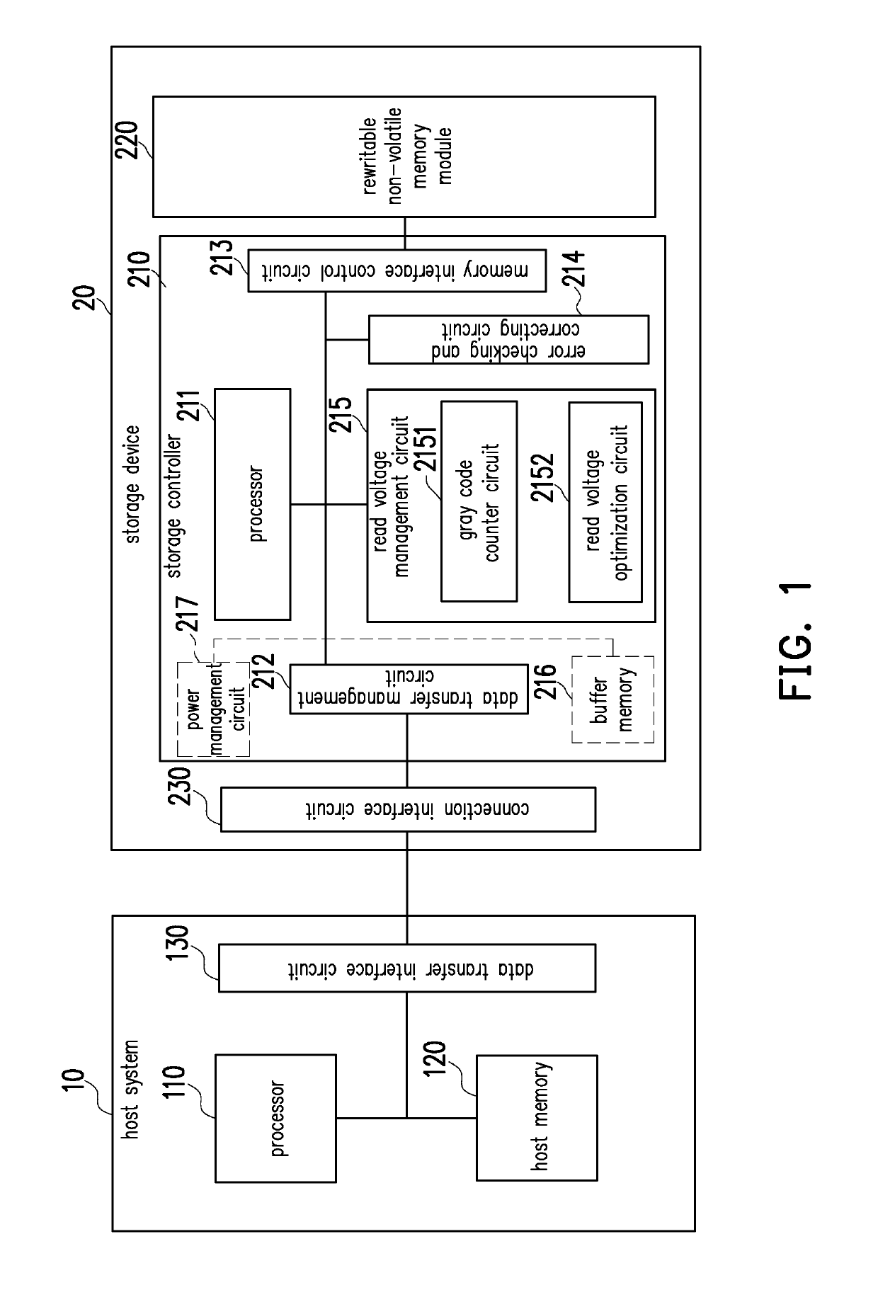
Figure 1 
Figure 2 
Figure 3
Abstract
Description
CROSS-REFERENCE TO RELATED APPLICATION
[0001] This application claims the priority benefit of Taiwan application serial no. 107108154, filed on Mar. 9, 2018. The entirety of the above-mentioned patent application is hereby incorporated by reference herein and made a part of this specification.BACKGROUND OF THE INVENTIONField of the Invention
[0002] The invention relates to a decoding method, and particularly relates to a decoding method and a storage controller for a storage device having a rewritable non-volatile memory module.Description of Related Art
[0003] In general, when data is read from a rewritable non-volatile memory module, if a page reading failure does not occur, the system may read the data based on a default read voltage set or an optimal read voltage set used previously. When a read failure occurs, the system (storage system) may stop using the default read voltage set or the optimal voltage used previously and correspondingly adjust the read voltage set.
[0004] In other wo...
Examples
Embodiment Construction
[0026]In the present embodiment, a storage device includes a rewritable non-volatile memory module and a storage device controller (which is also referred to as a storage controller or a storage control circuit). Moreover, the storage device is used together with a host system, and the host system may write data into the storage device or read data from the storage device.
[0027]FIG. 1 is a block diagram of a host system and a storage device according to an embodiment of the invention.
[0028]Referring to FIG. 1, the host system 10 includes a processor 110, a host memory 120 and a data transfer interface circuit 130. In the present embodiment, the data transfer interface circuit 130 is coupled (i.e., electrically connected to) the processor 110 and the host memory 120. In another embodiment, the processor 110, the host memory 120 and the data transfer interface circuit 130 are coupled to each other through a system bus.
[0029]The storage device 20 includes a storage controller 210, a re...