
Process for fabricating at least one tensilely strained planar photodiode
a technology of planar photodiodes and tensile strain, which is applied in the direction of photometry using electric radiation detectors, electrical apparatus, and semiconductor devices, etc., can solve the problems of difficult control of the value of the tensile strain experienced by the semiconductor layer, the complexity of the fabrication process, and the drawback of being obtained using a relative complex fabricating process
Patent Information
- Authority / Receiving Office
- US · United States
- Patent Type
- Patents(United States)
- Current Assignee / Owner
- Publication Date
- 2022-11-22
Smart Images
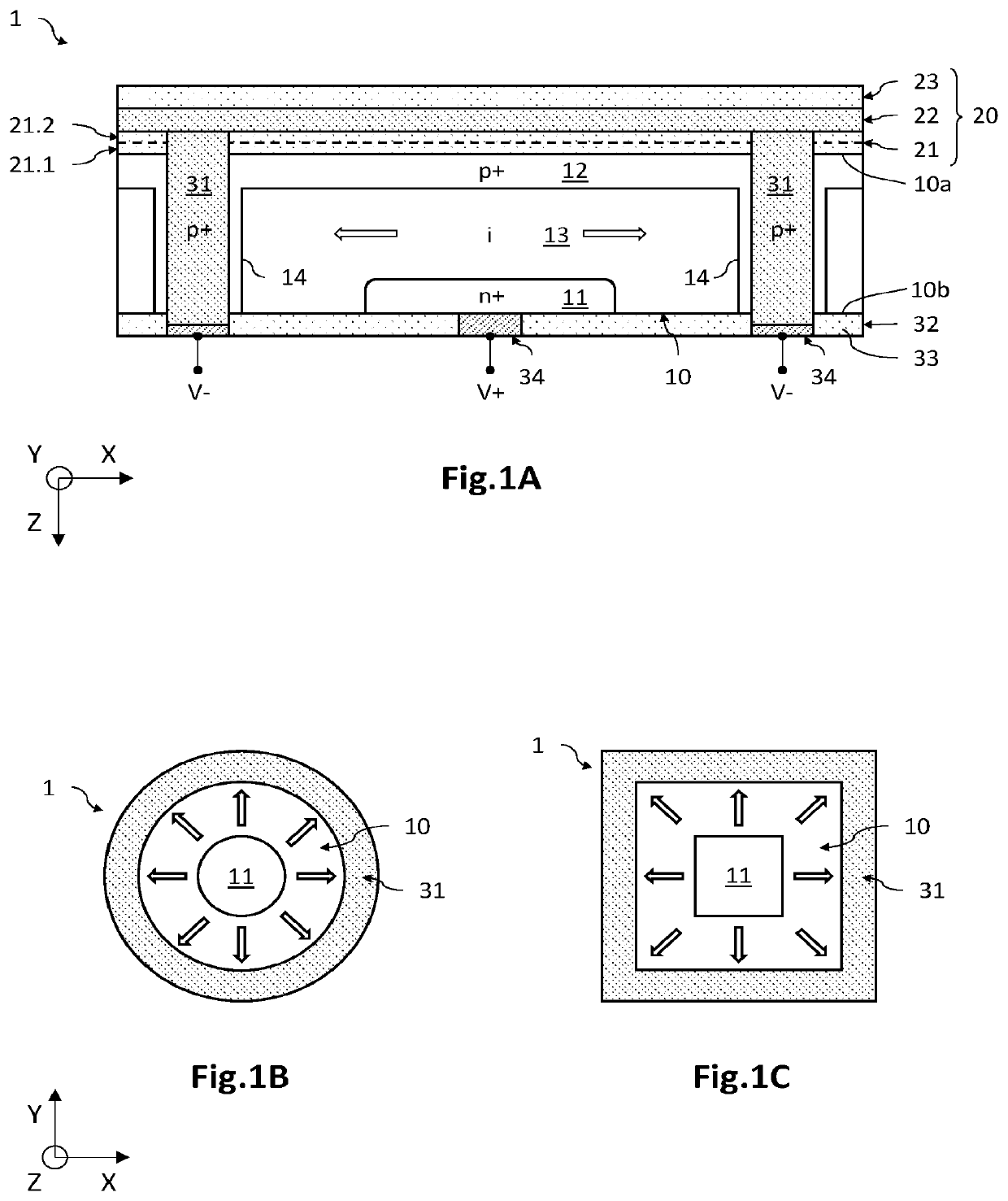
Figure 1 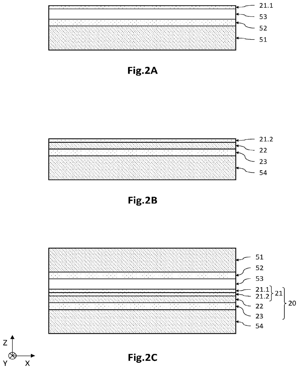
Figure 2 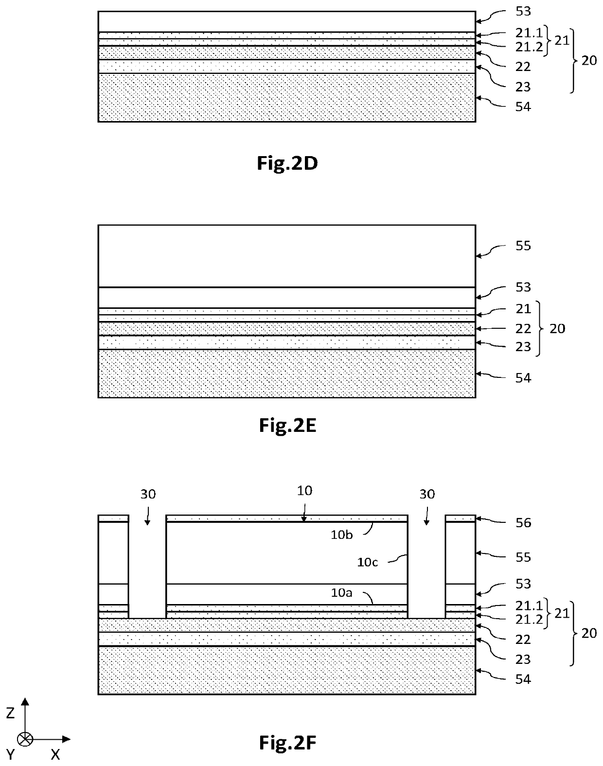
Figure 3
Abstract
Description
TECHNICAL FIELD
[0001] The field of the invention is that of optoelectronic devices comprising at least one planar photodiode made based on a tensilely strained semiconductor compound and for example based on germanium. The invention is notably applicable to the field of detection of light radiation belonging for example to the near infrared, for example in the field of optical telecommunications and infrared imaging.PRIOR ART
[0002] In various microelectronic or optoelectronic applications, it may be advantageous to use a layer made of a crystalline, and preferably single-crystal, semiconductor compound having a tensile mechanical strain. This is notably the case in certain optical devices the material of the optically active layer of which has, unstrained, an indirect electronic band structure, the band structure then being made direct by applying a sufficient tensile strain. The crystalline semiconductor compound may be a compound based on germanium, for example germanium, germanium-...
Examples
Embodiment Construction
[0034]In the figures and in the following description, the same references represent identical or similar elements. In addition, the various elements are not shown to scale for the sake of clarity of the figures. Furthermore, the various embodiments and variants are not mutually exclusive and may be combined with one another. Unless otherwise indicated, the terms “substantially”, “about” and “of the order of” mean to within 10%, and preferably to within 5%. In addition, the terms “comprised between . . . and . . . ” and equivalents mean inclusive of limits, unless otherwise specified.
[0035]The invention notably relates to a process of fabricating at least one planar photodiode, and preferably a matrix array of planar photodiodes. Each photodiode is preferably suitable for detecting light radiation in the near infrared (SWIR, for Short Wavelength IR) corresponding to the spectral range extending from 0.8μm to about 1.7 μm, or even to about 2.5 μm, and is preferably made based on germ...