
Electronic package of photo-image sensors in cellular phone camera modules, and the fabrication and assembly thereof
Patent Information
- Authority / Receiving Office
- US · United States
- Current Assignee / Owner
- Publication Date
- 2005-04-07
Smart Images

Figure 1 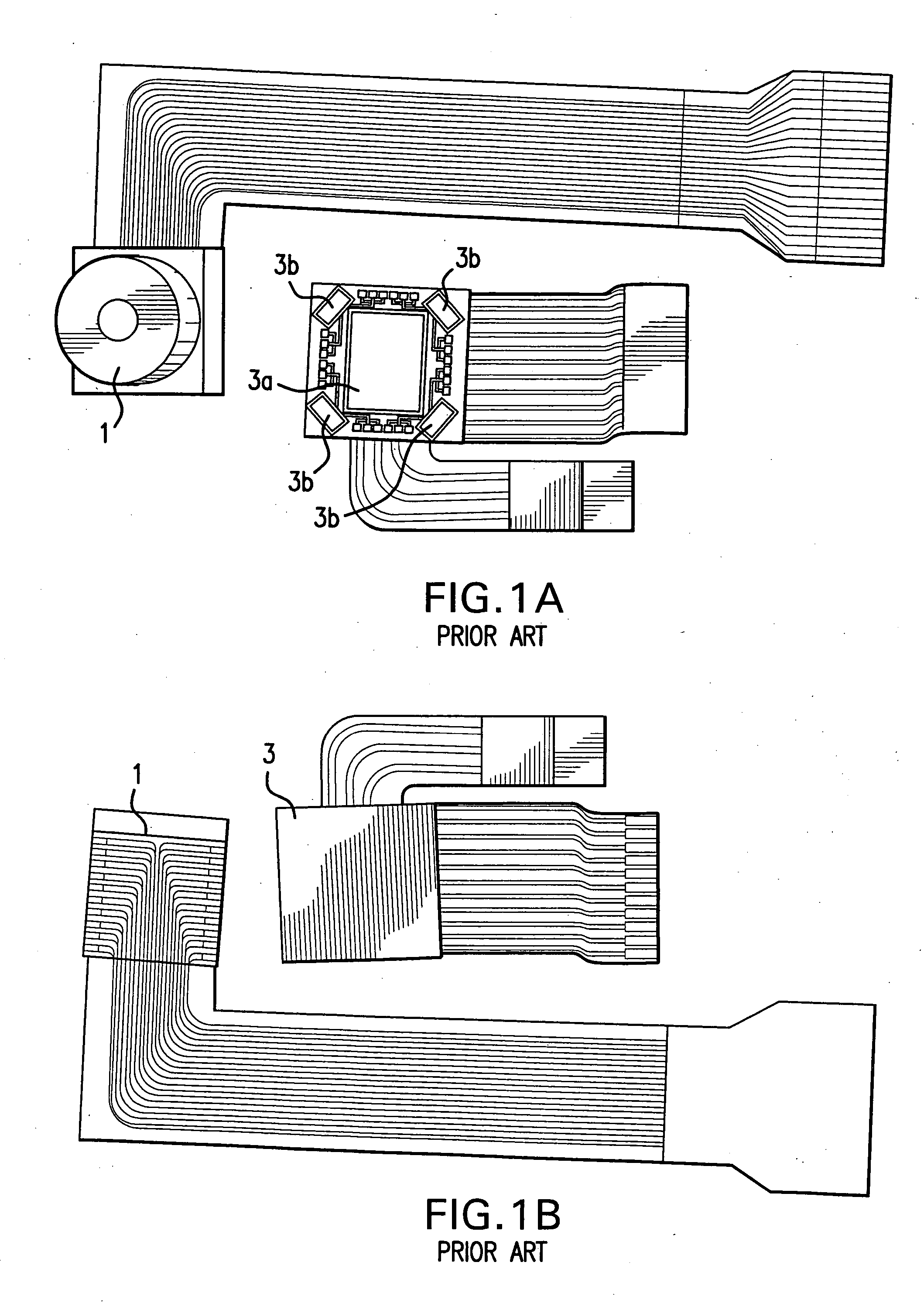
Figure 2 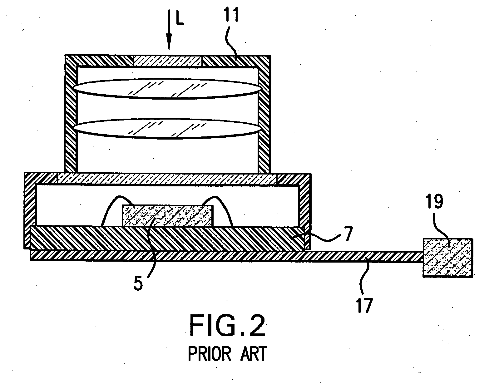
Figure 3
Abstract
Description
RELATED U.S. APPLICATION DATA
[0001] This Application is based on U.S. Provisional Patent Application Ser. No. 60 / 536,536, filed 15 Jan. 2004. This Application is a Continuation-In-Part of co-pending U.S. Non-provisional patent application Ser. No. 10 / 692,816, filed 23 Oct. 2003, which is based on U.S. Provisional Patent Application Ser. No. 60 / 507,100, filed 1 Oct. 2003.BACKGROUND OF THE INVENTION
[0002] 1. Field of the Invention
[0003] The present invention relates generally to electronic packaging of semiconductor integrated circuits, and particularly, to electronic packaging of photo-sensing semiconductor devices. More specifically, the present invention relates to electronic packaging of photo image sensors in such compact applications as cellular telephone camera modules.
[0004] 2. Prior Art
[0005] FIGS. 1A, 1B illustrate top and bottom views of typical camera modules 1, 3 often employed in cellular telephones. In the smaller of the modules 3, the lens housing is removed to mor...
Examples
Embodiment Construction
[0047] A photo-sensing semiconductor wafer has a plurality of dice, and each die has integrated circuitry formed on a front surface of the wafer, much as in other semiconductor wafers. Each die has a plurality of bonding pads. The wafer has a patterned passivation layer over the front surface for protecting the integrated circuitry underneath. The passivation layer has openings on said bonding pads. Each such photo-sensing die has at least one photo-sensing area on a front surface.
[0048] Wafer bumping is a well-known technique that has been widely used since its initial teaching, as reflected in U.S. Pat. No. 3,292,240 entitled “Method of Fabricating Microminiature Functional Components,” assigned to IBM. A typical wafer bumping process includes at least one patterned metal layer for making solder bump pads connected to bonding pads on the wafer. Metallurgy used for solder bump pads is commonly referred to as under bump metallurgy (UBM) and typically utilizes a multilayered structu...