
Orientated group IV-VI semiconductor structure, and method for making and using the same
a technology of semiconductor structure and orientated group, which is applied in the direction of lasers, bulk negative resistance effect devices, semiconductor lasers, etc., can solve the problems of limited tuning range and performance of vcsels, and the performance of these vcsels remains far from the desired level, so as to achieve the effect of improving performan
Patent Information
- Authority / Receiving Office
- US · United States
- Patent Type
- Applications(United States)
- Current Assignee / Owner
- Publication Date
- 2005-09-15
- Estimated Expiration
- Not applicable · inactive patent
Smart Images
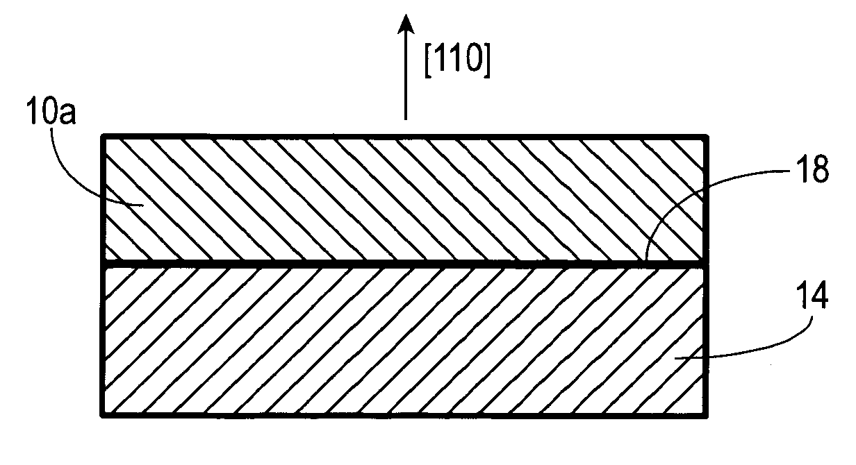
Figure 1 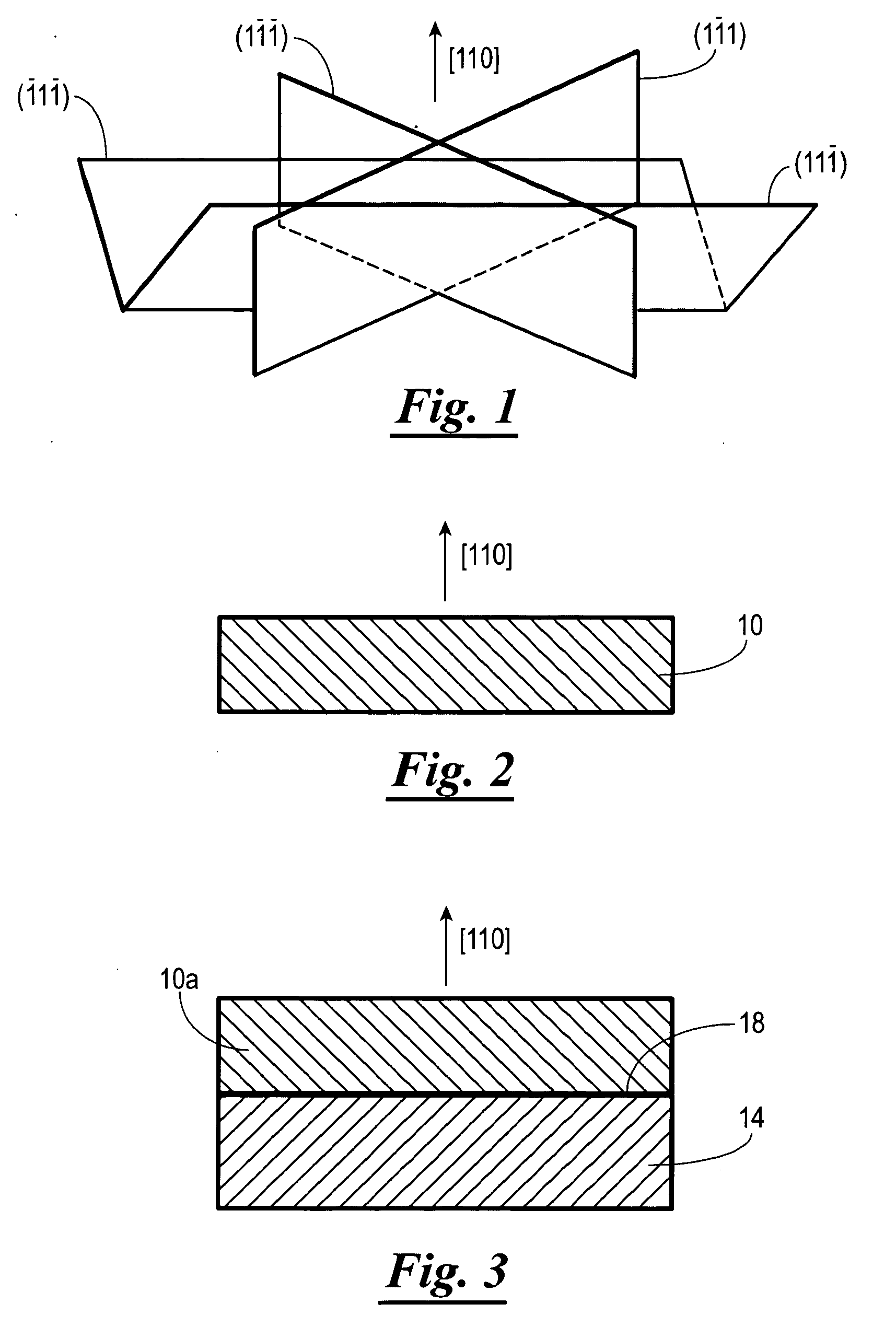
Figure 2 
Figure 3
Abstract
Description
CROSS-REFERENCE TO RELATED APPLICATIONS
[0001] The present application claims priority to the provisional patent application identified by the U.S. Ser. No. 60 / 542,023, which was filed on Feb. 5, 2004, the entire content of which is hereby expressly incorporated herein by reference.STATEMENT REGARDING FEDERALLY SPONSORED RESEARCH OR DEVELOPMENT
[0002] Research regarding one or more portions of the present invention may have been funded pursuant to DOD ARO Grant Number DAAD19-03-1-0313.BACKGROUND OF THE INVENTION
[0003] IV-VI lead salt semiconductors have wide spread applications for devices such as mid-infrared lasers, detectors and thermal electrical cooling devices. Previously, these devices have been fabricated using either
[100] or
[111] substrates such as
[100] IV-VI substrates,
[111] BaF2 substrates and
[111] Si substrates. Efforts have also been made to fabricate devices on III-V GaAs, GaSb substrates and II-VI CdTe, CdSe substrates.
[0004] In the area of lasers, much of the ...
Examples
Embodiment Construction
[0024] Generally, the present invention relates to a IV-VI group semiconductor structure having a [110] orientation, and a method for making and using the same. The [110] orientation of the group IV-VI semiconductor structure of the present invention offers some advantages over other orientations. Shown in FIG. 1 is a schematic representation of the geometry of [110] surfaces in a diamond cubic semiconductor material with the {111} planes shown. For example, a IV-VI lead salt semiconductor material having a rock salt structure would belong to the diamond cubic group. Also, shown in Table 1 below is the effective mass for different orientations for the energy minima shown in FIG. 1. For PbSe, ml≈2mt.
TABLE 1Effective masses along differentorientations for L-valley energy minimaSurfaceOrientationmxmymzDegeneracy{100}mt+2ml33mtmlmt+2ml4{110}mtml+2mt33mtmlml+2mt2mtmlml2{111}mtml1mtmt+8ml99mtmlmt+8ml3
[0025] The [110] orientation of the group IV-VI semiconductor structure of ...