
Semiconductor device
a semiconductor and device technology, applied in semiconductor lasers, instruments, optical elements, etc., can solve the problems of non-trivial monolithic integration of iii-v based light sources on silicon platforms, time-consuming and difficult to achieve relatively high-precision alignment, and achieve easy integration/implementation, widening a range of applications/optical systems, and easy fabrication and/or integration.
Patent Information
- Authority / Receiving Office
- US · United States
- Patent Type
- Patents(United States)
- Current Assignee / Owner
- Publication Date
- 2016-12-06
Smart Images
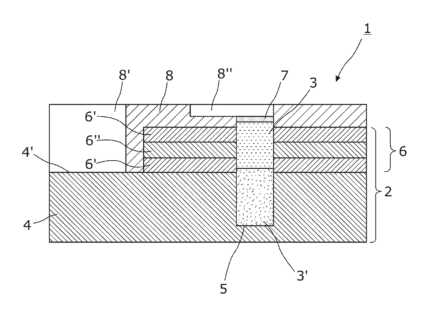
Figure 1 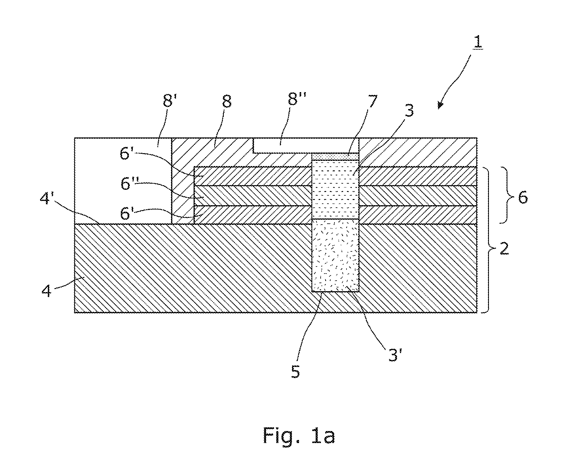
Figure 2 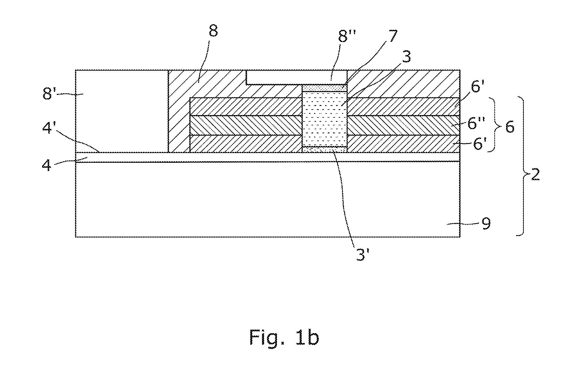
Figure 3
Abstract
Description
CROSS-REFERENCE TO RELATED APPLICATIONS
[0001] This application is based on and claims the benefit of priority of the filing date of commonly-owned, co-pending on PCT Application No. PCT / IB2013 / 059814 filed Oct. 31, 2013, which further claims the benefit of priority from commonly-owned Great Britain Patent Application 1219595.4, filed on Oct. 31, 2012.FIELD OF THE INVENTION
[0002] The present invention relates to a semiconductor device for use in an optical application and a method of fabrication therefor.BACKGROUND OF THE INVENTION
[0003] In order to meet the requirements of future computing systems, higher speed and more energy efficient alternatives to electrical interconnects such as, for example, on-chip optical interconnects and chip-to-chip optical interconnects, may be needed. Integrated optics, particularly silicon photonics, may suitably meet such needs. For the cost-effective, mass-fabrication of complementary metal-oxide semiconductor (CMOS)-based chips having a performance ca...
Examples
Embodiment Construction
[0060]Within the description, the same reference numerals or signs have been used to denote the same parts or the like.
[0061]Reference is now made to FIG. 1a showing a semiconductor device 1 according to an embodiment of a first aspect of the present invention comprising at least an optically passive aspect or region 2 that, when the semiconductor device 1 is in use, is operable in substantially an optically passive mode for the transmission and / or coupling of light from a given location to a desired location, rather than for the generation, amplification, detection and / or modulation of light. The optically passive aspect 2 is structured thereby to comprise at least a predefined structure 5, which extends to at least an upper surface 4′ of a crystalline seed layer 4 provided in respect of the optically passive aspect 2 or even into the crystalline seed layer 4 as for a given embodiment of the present invention as shown in FIG. 1a. There is also provided at least an optically active ...