
Semiconductor devices having bonded interfaces and methods for making the same
Patent Information
- Authority / Receiving Office
- US · United States
- Current Assignee / Owner
- Publication Date
- 2005-12-22
- Estimated Expiration
- Not applicable · inactive patent
Smart Images
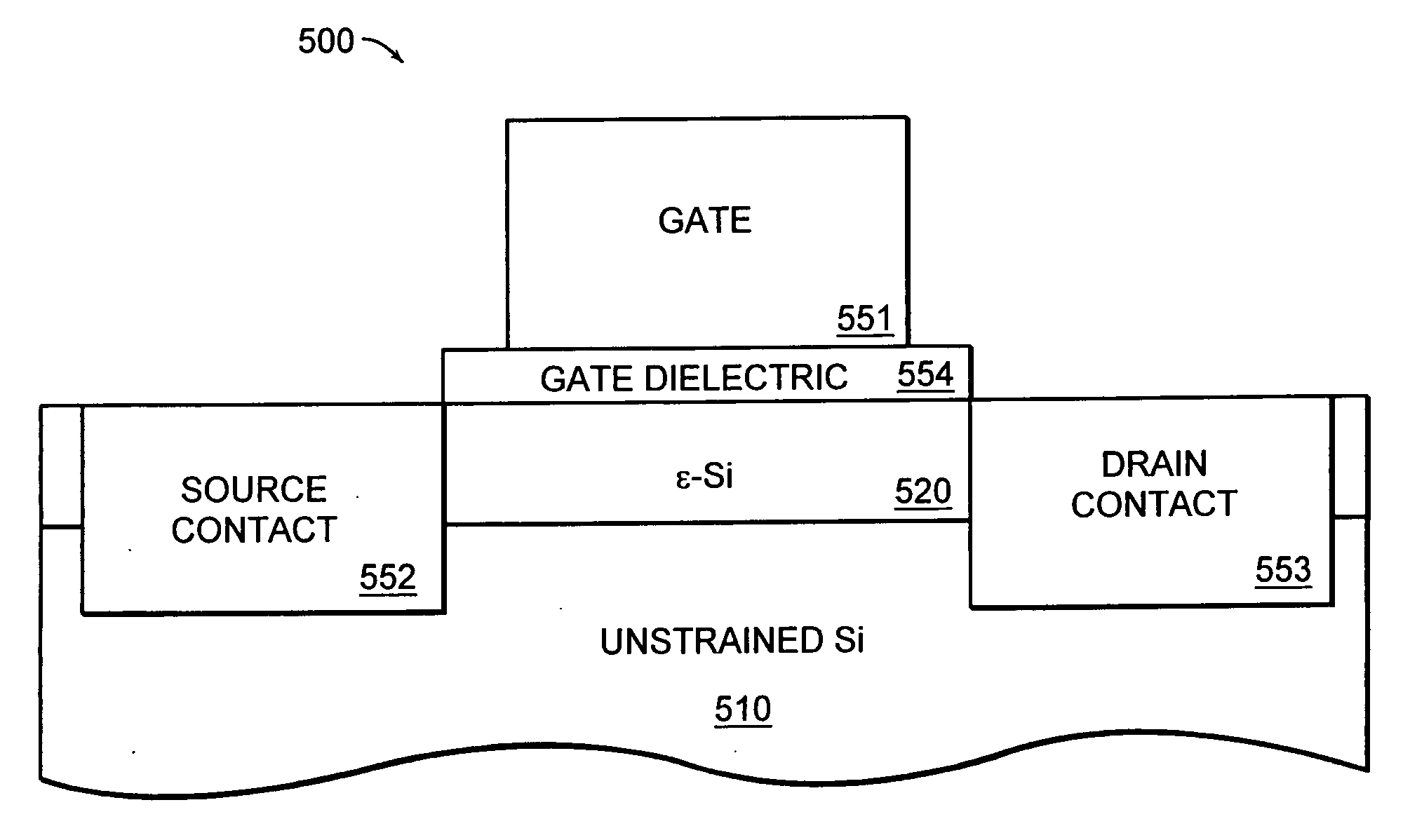
Figure 1 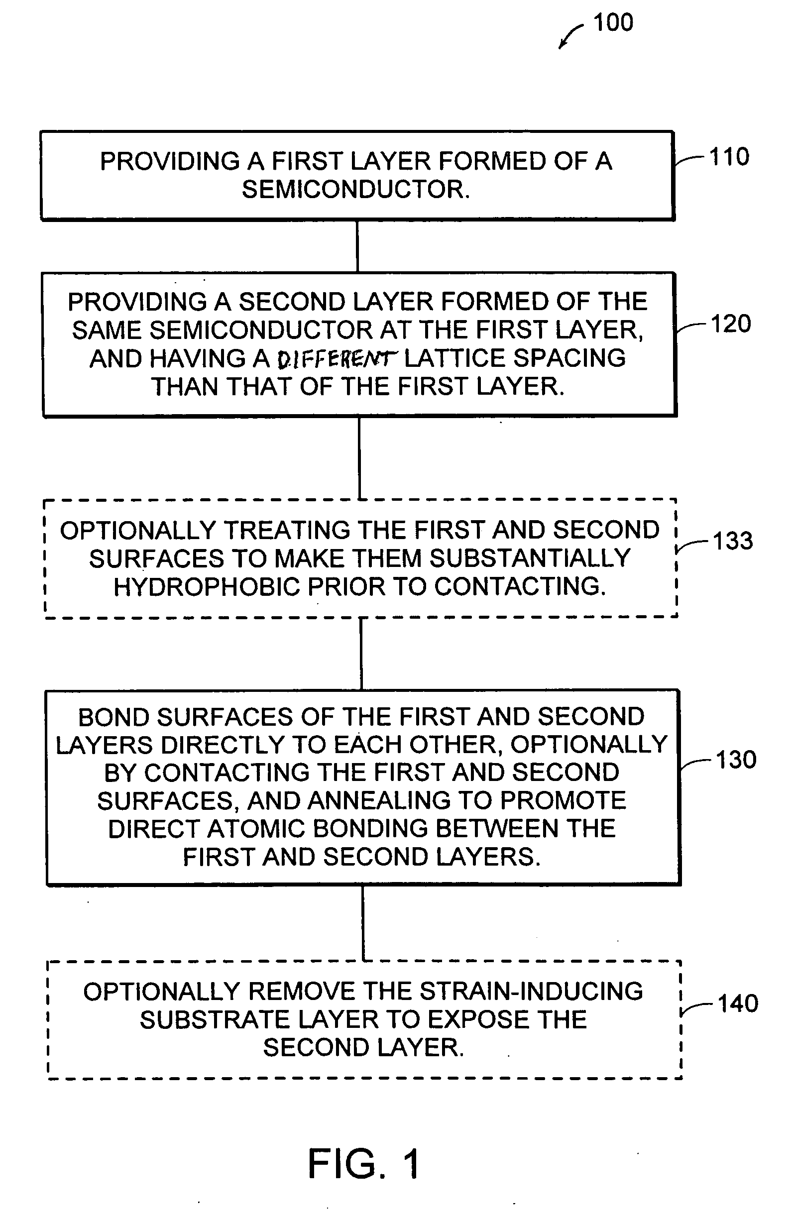
Figure 2 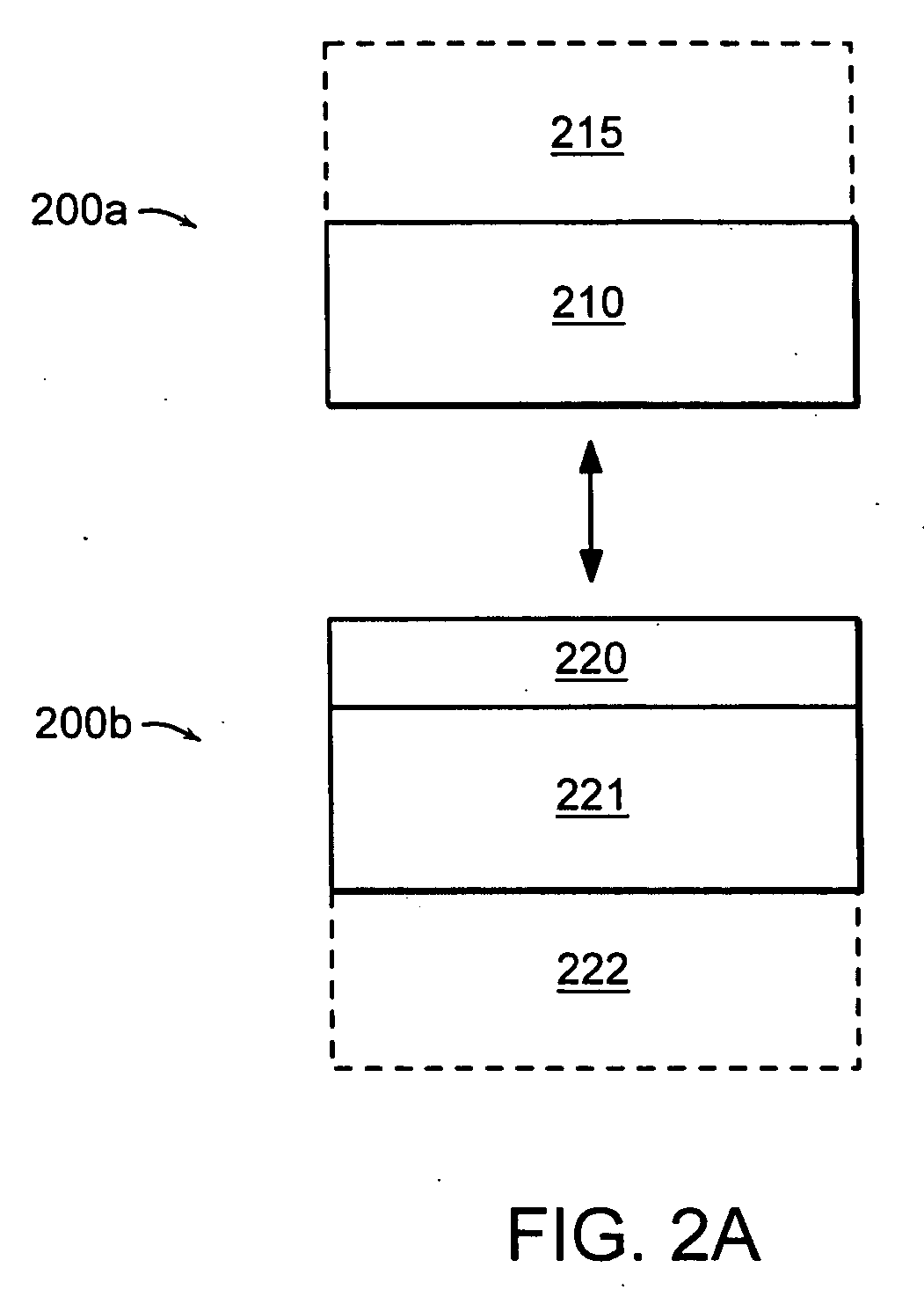
Figure 3
Abstract
Description
RELATED APPLICATIONS
[0001] This application is a Continuation-in-Part of application Ser. No. 10 / 869,463, filed Jun. 16, 2004, which is incorporated herein by reference.BACKGROUND OF INVENTION
[0002] 1. Field of Invention
[0003] The invention relates to semiconductor-based electronic devices, and, more particularly, to the structure and fabrication of semiconductor-based substrates and electronic devices that include strained semiconductor layers.
[0004] 2. Discussion of Related Art
[0005] Some advanced semiconductor-based devices include a semiconductor layer that is strained by application of a stress to provide improved performance of the devices. For example, metal-oxide-semiconductor (MOS) transistors having a channel formed in strained silicon or strained Si1-yGey formed on unstrained, or relaxed, Si1-xGex, can exhibit improved carrier mobility in comparison to traditional p-type MOS (PMOS) and n-type MOS (NMOS) transistors. Strained-layer MOS transistors can be formed on “vi...
Examples
Embodiment Construction
[0024] This invention is not limited in its application to the details of construction and the arrangement of components set forth in the following description or illustrated in the drawings. The invention is capable of other embodiments and of being practiced or of being carried out in various ways. Also, the phraseology and terminology used herein is for the purpose of description and should not be regarded as limiting. The use of “including,”“comprising,” or “having,”“containing,”, “involving,” and variations thereof herein, is meant to encompass the items listed thereafter and equivalents thereof as well as additional items.
[0025] The term “MOS” is used herein to refer generally to semiconductor devices that include a conductive gate spaced at least by an insulating layer from a semiconducting channel layer. The terms “SiGe” and “Si1-xGex” are used in this description, depending on context, to interchangeably refer to silicon-germanium alloys. The term “silicide” is used in thi...