
Circuit and method for detecting pixel defect
a technology of defect detection and circuit, applied in the field of imaging devices, can solve the problems of increased production cost, new pixel defect due to ageing deterioration, unreachable, etc., and achieve the effects of high-accuracy pixel defect detection, low cost circuitry, and simple circuitry
Patent Information
- Authority / Receiving Office
- US · United States
- Patent Type
- Applications(United States)
- Current Assignee / Owner
- Publication Date
- 2006-06-15
- Estimated Expiration
- Not applicable · inactive patent
Smart Images
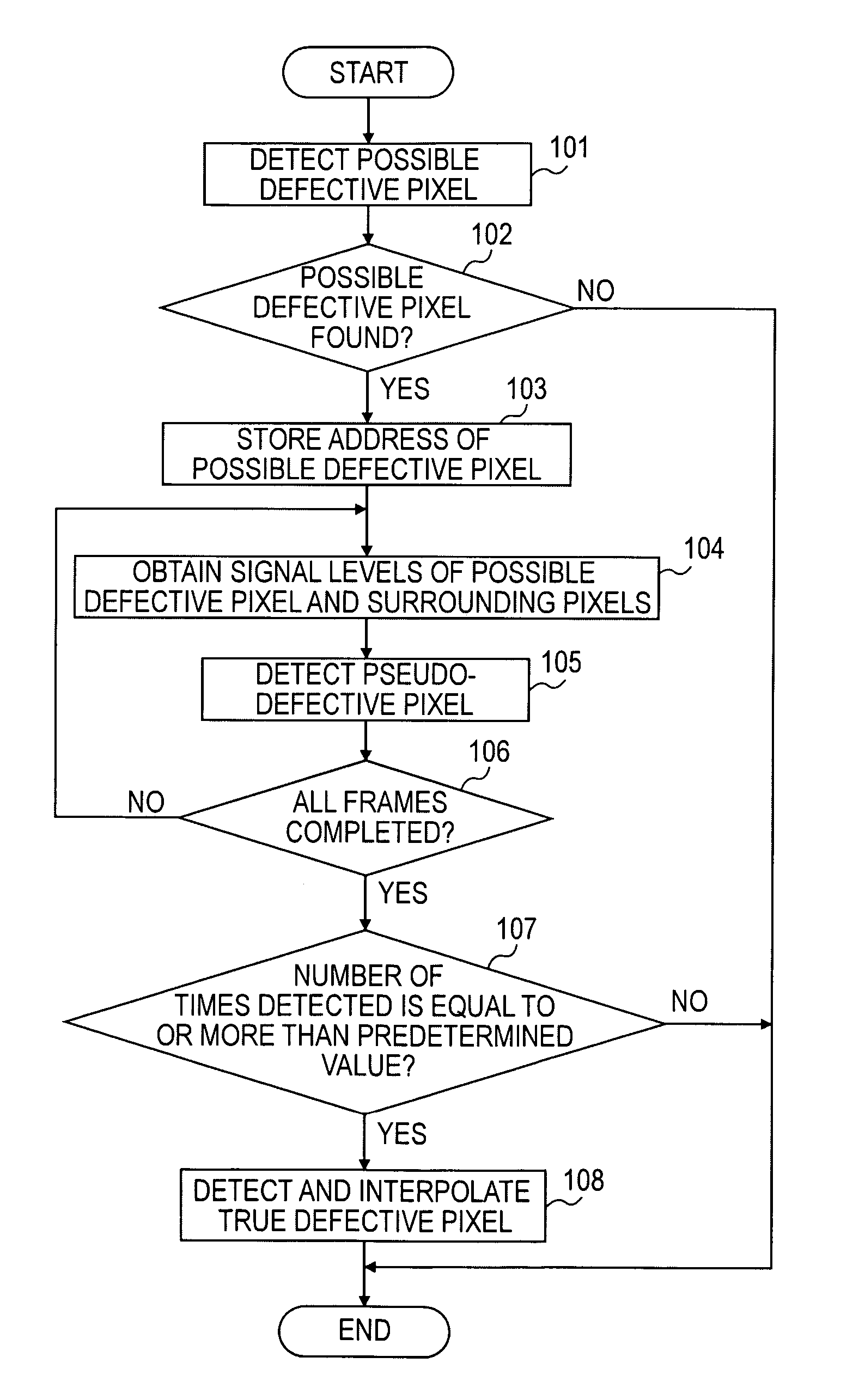
Figure 1 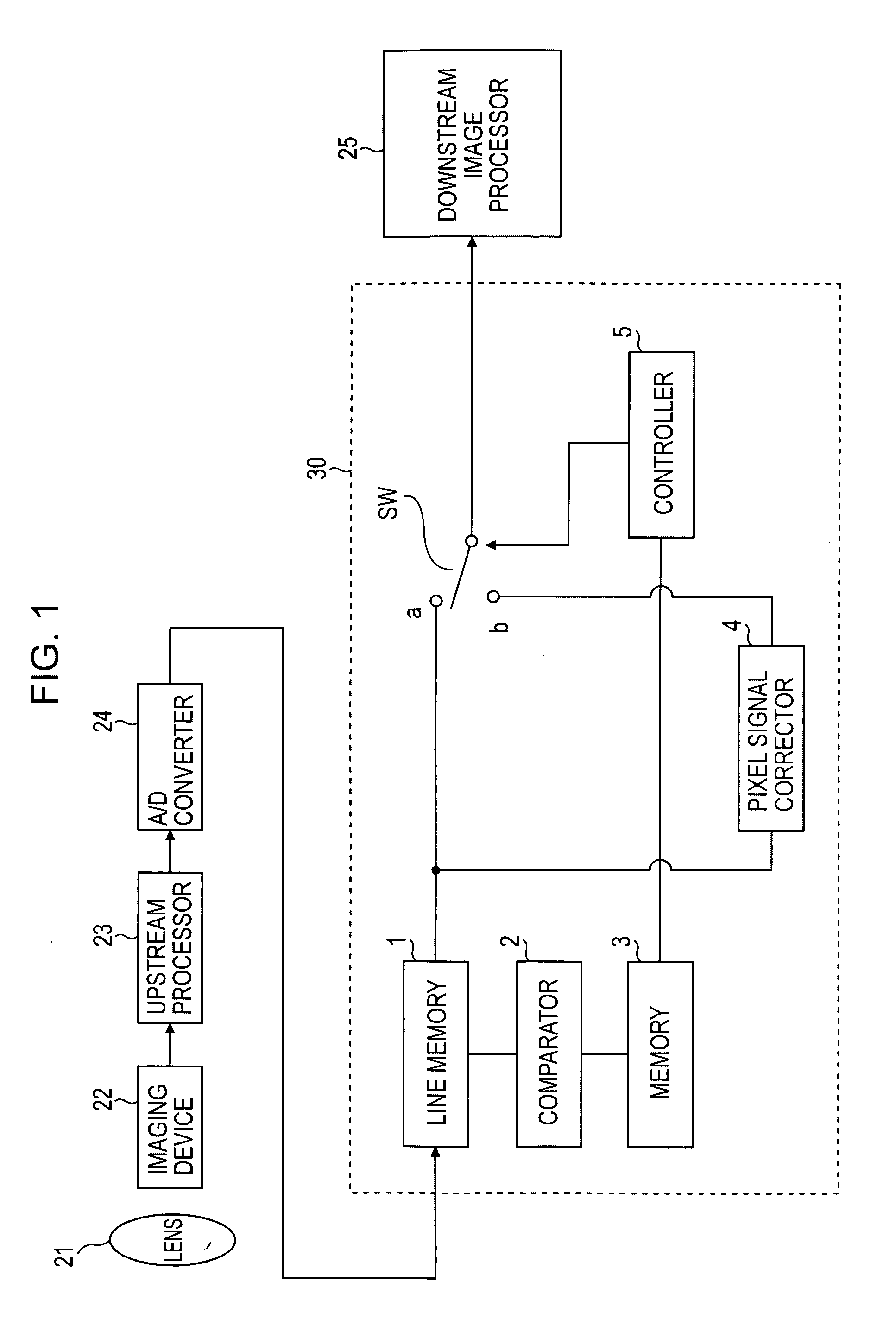
Figure 2 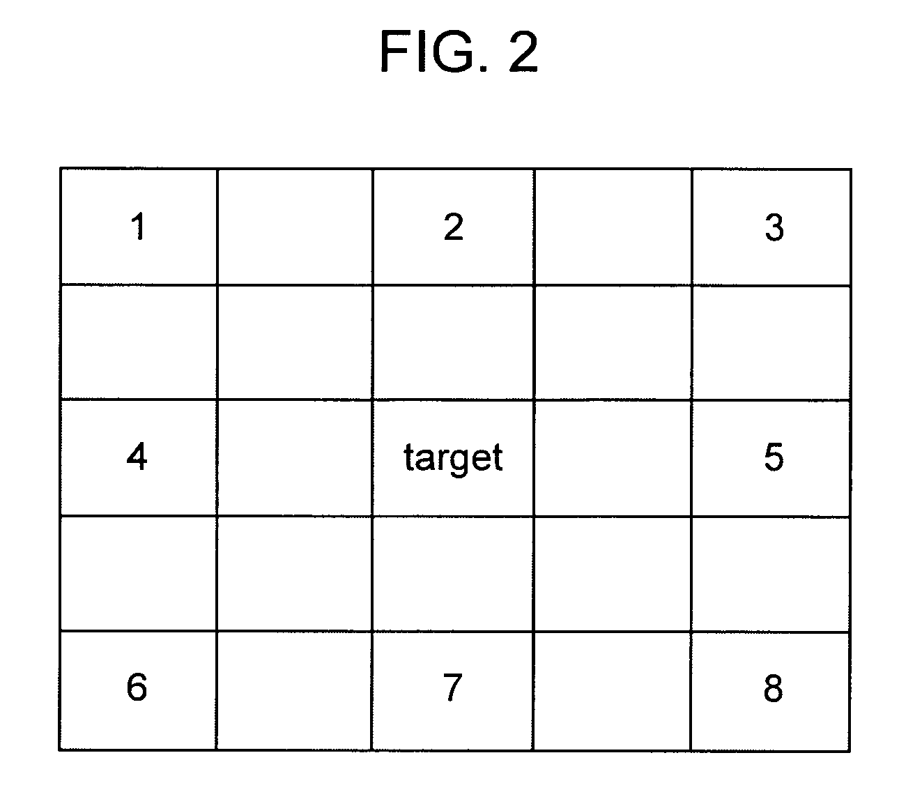
Figure 3
Abstract
Description
CROSS REFERENCES TO RELATED APPLICATIONS
[0001] The present invention contains subject matter related to Japanese Patent Application JP 2004-356473 filed in the Japanese Patent Office on Dec. 9, 2004, the entire contents of which are incorporated herein by reference. BACKGROUND OF THE INVENTION
[0002] 1. Field of the Invention
[0003] The present invention relates to imaging devices. More specifically, the present invention relates to a pixel defect detecting circuit and method for use in solid-state imaging devices, such as charge-coupled devices (CCDs), for detecting pixel defects.
[0004] 2. Description of the Related Art
[0005] Solid-state imaging devices, such as CCDs, typically detect and correct for image display errors, such as white defects. A white defect occurs such that a video signal region having a high signal level due to a crystal defect of a semiconductor device causes a higher brightness than an image portion therearound to bring a white pixel condition.
[0006] In a ...
Examples
Embodiment Construction
[0017] A pixel defect of an imaging device is automatically detected with simple, low-cost circuitry in the following way. Pixel signals on one horizontal line are input from the imaging device, and a level of a target pixel signal is compared with levels of a plurality of surrounding pixel signals located to the right and left of the target pixel signal. If a difference between the levels is higher than a threshold value, the pixel corresponding to the target pixel signal is detected as a possible defective pixel, and the address of the detected possible defective pixel is held. After holding the levels of the detected possible defective pixel signal and the surrounding pixel signals from the pixel signals in the next frame, a correlation between the possible defective pixel signal and the surrounding pixel signals is calculated. If the correlation is not found, the possible defective pixel is detected as a pseudo-defective pixel, and the detection of the pseudo-defective pixel is ...