
End point detection in workpiece processing
a technology for workpieces and end points, applied in the field of workpiece processing, can solve the problems of affecting the accuracy of end point detection, and wasting time and process chemicals, and achieve the effect of improving accuracy and reducing optical nois
Patent Information
- Authority / Receiving Office
- US · United States
- Patent Type
- Applications(United States)
- Current Assignee / Owner
- Publication Date
- 2007-05-31
Smart Images
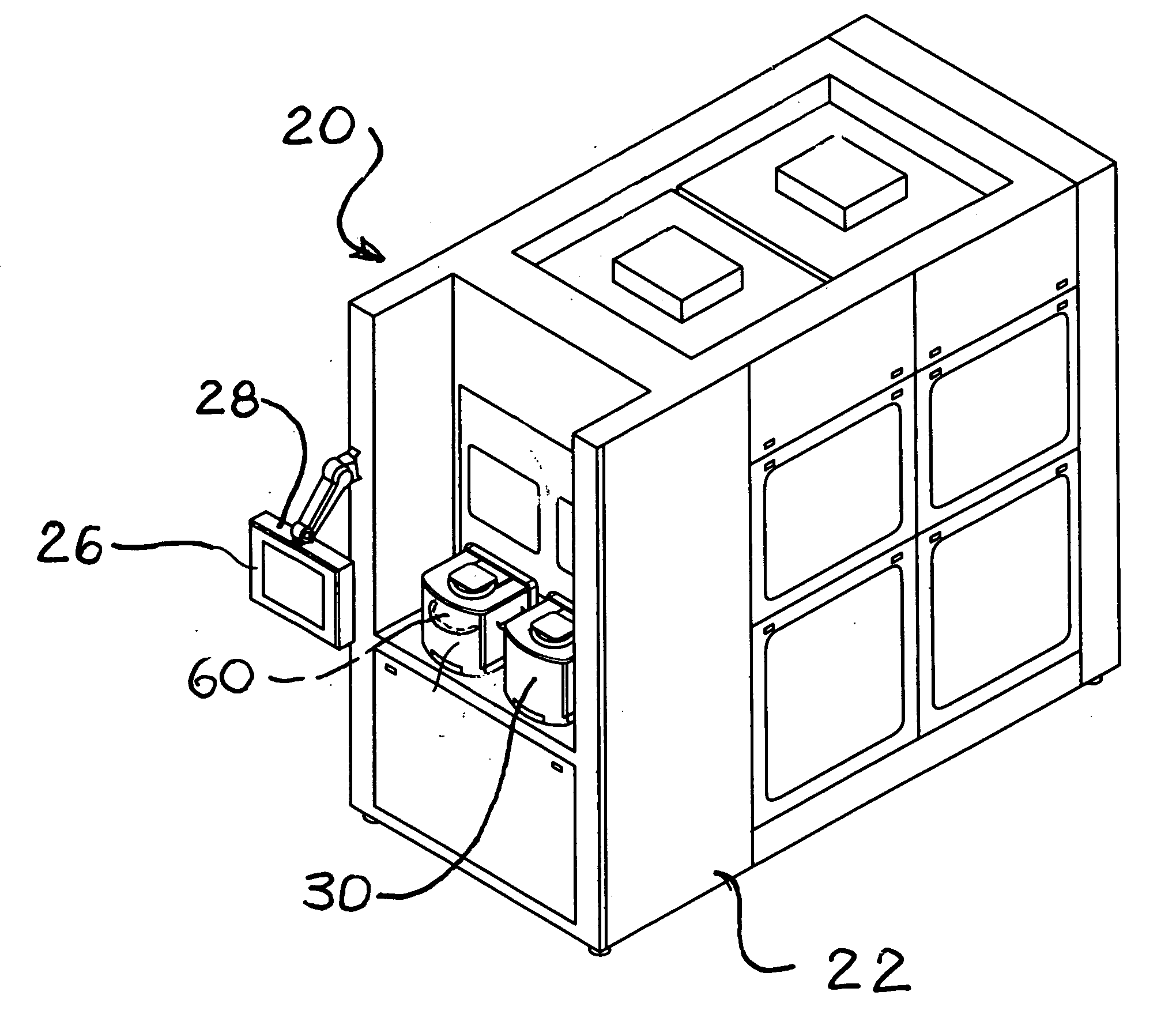
Figure 1 
Figure 2 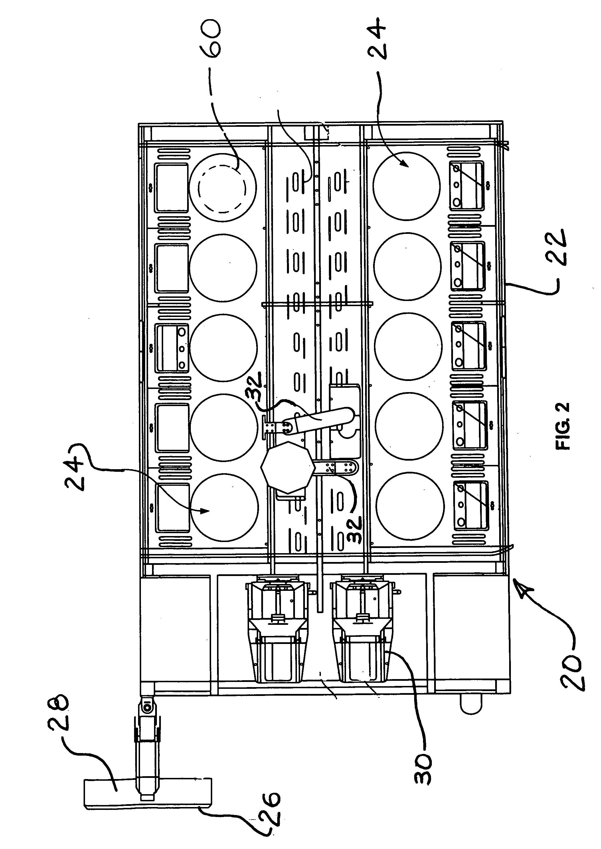
Figure 3
Abstract
Description
BACKGROUND OF THE INVENTION
[0001] The invention relates to processing of workpieces, such as semiconductor wafers. Semiconductor and similar microscale devices are typically manufactured by performing many separate steps on substrates or wafers. The workpieces are often coated or plated with multiple layers or films of different materials. Process chemicals, typically etchants in liquid form, are applied to the workpieces to selectively remove one or more layers. Often, a layer on the workpiece is patterned generally using photolithographic methods, and only portions of the layer are removed.
[0002] In workpiece processing, it is often important to determine the end point of a process. In a layer or film removal process, the end point is defined as the point at which all of the targeted layer has been removed, exposing an underlying layer beneath the targeted layer. Extensive processing after the end point can waste time and process chemicals, and even damage the workpiece in more ...
Examples
Embodiment Construction
[0021] The systems and methods described may be used to process workpieces, such as semiconductor wafers, flat panel displays, hard disk media, CD glass, memory and optical media, MEMS devices, and various other substrates on which micro-electronic, micro-mechanical, or micro-electromechanical devices are or can be formed. These are collectively referred to here as workpieces or wafers. Descriptions here of semiconductors, or the semiconductor industry or manufacturing processes, also includes the workpieces listed above, and their equivalents.
[0022] Turning now to the drawings, as shown in FIGS. 1 and 2, as one example, a processing system 20 includes one or more processors 24 within an enclosure 22. A control / display panel 26 is typically provided with the processing system 20, to allow system operators to monitor various operations, as well as entering or modifying system instructions and software. One or more computer controllers 28 is also typically provided with the processin...