
Chopper type comparator
Patent Information
- Authority / Receiving Office
- US · United States
- Current Assignee / Owner
- Publication Date
- 2007-12-06
- Estimated Expiration
- Not applicable · inactive patent
Smart Images
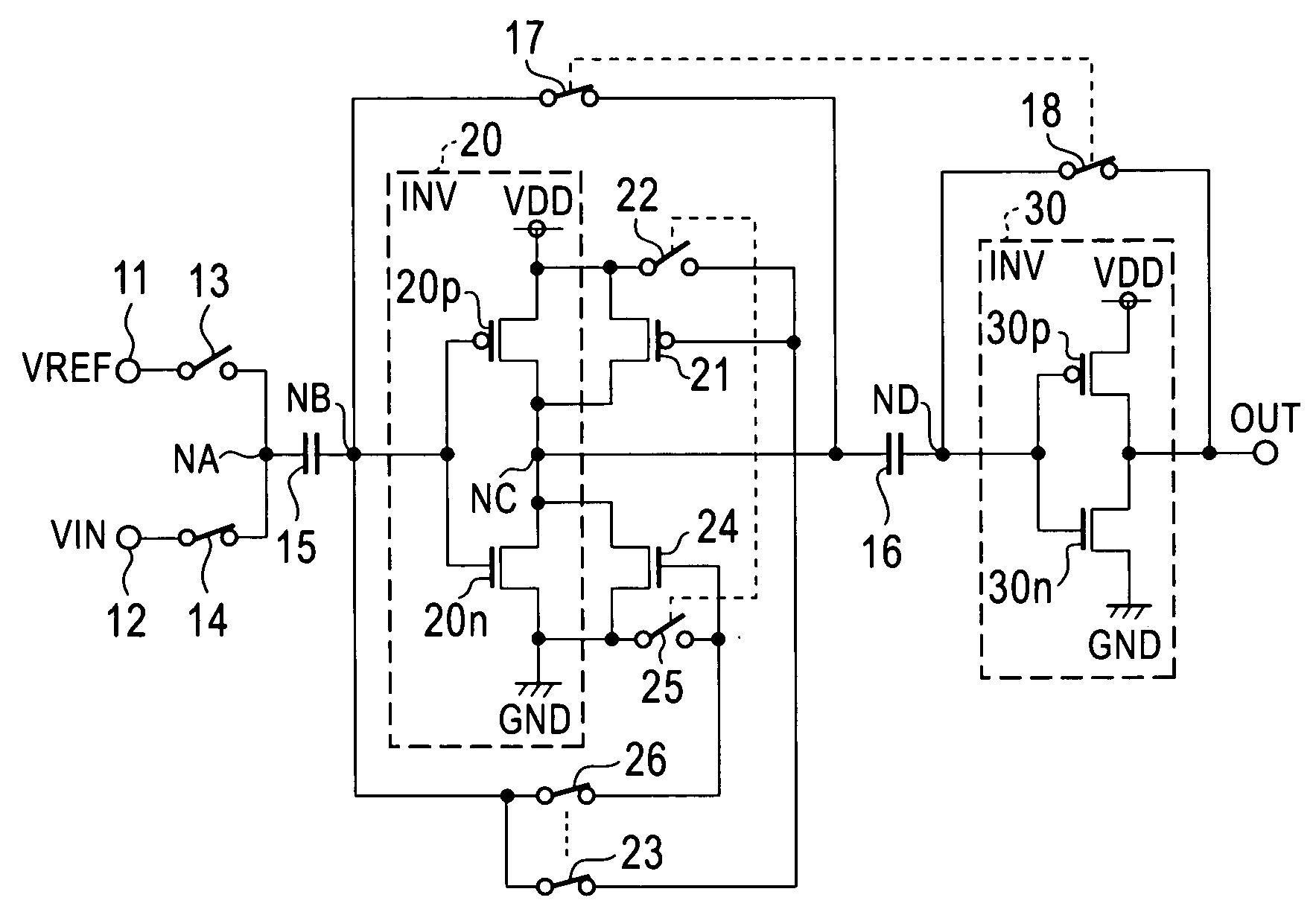
Figure 1 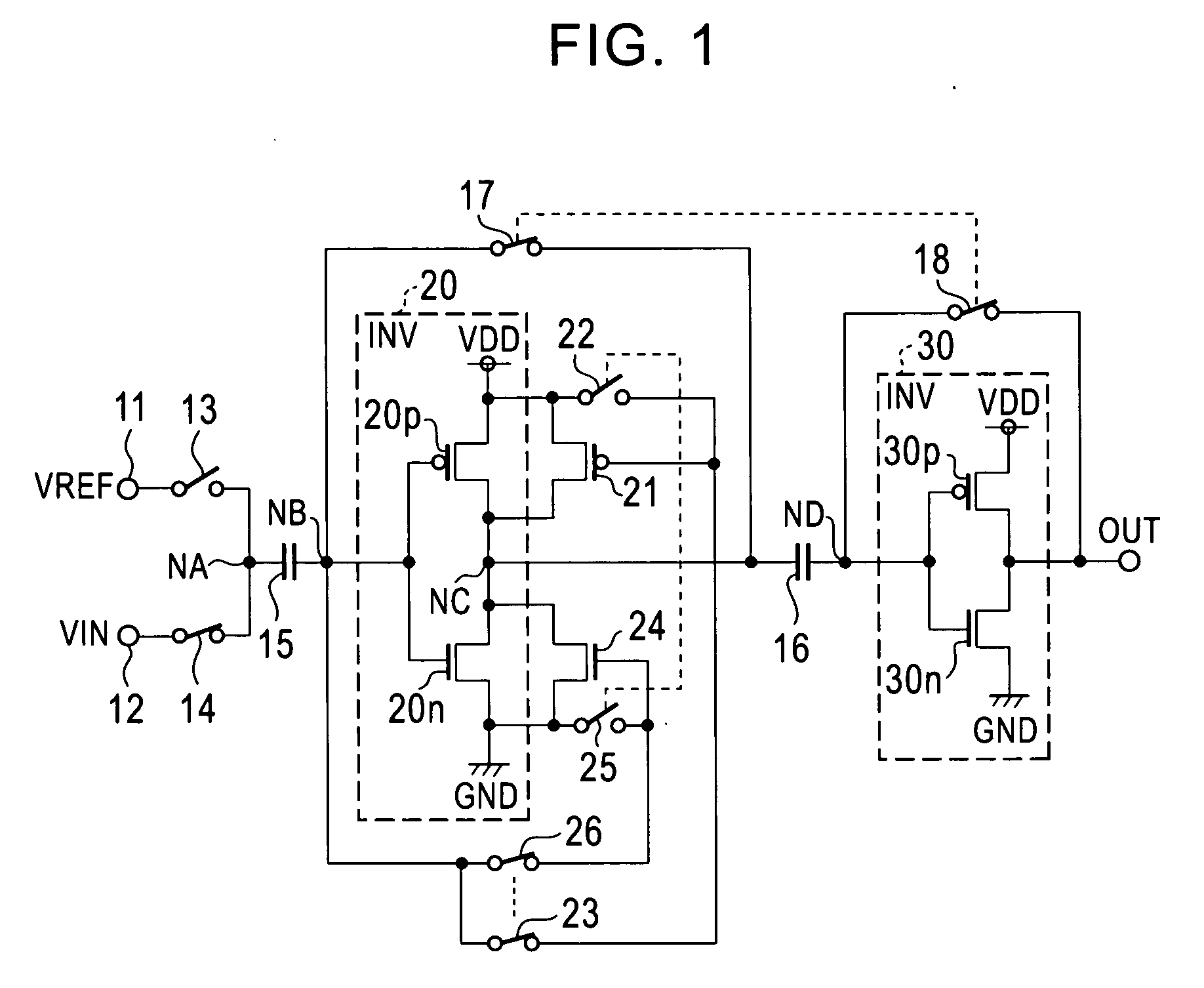
Figure 2 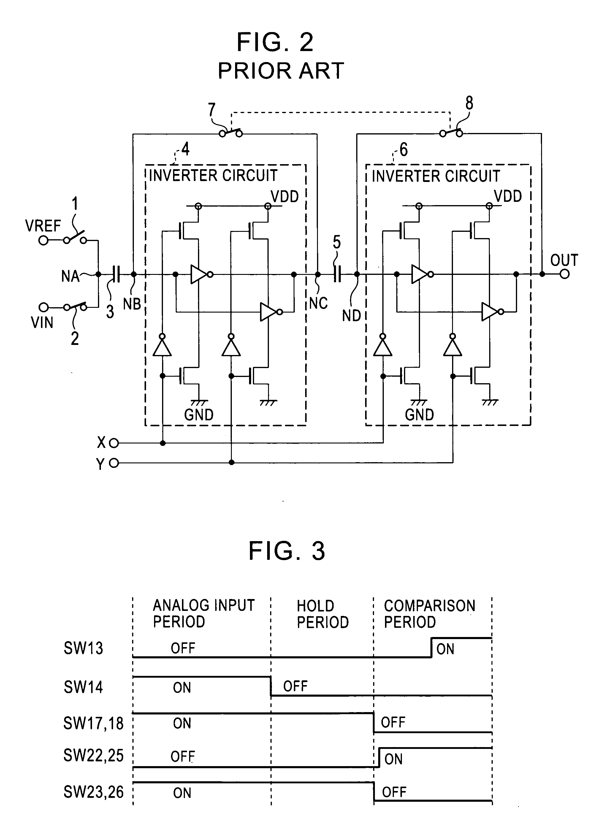
Figure 3
Abstract
Description
BACKGROUND OF THE INVENTION
[0001] 1. Field of the Invention
[0002] The present invention relates to a chopper type comparator used for an analog-to-digital converter, etc.
[0003] 2. Description of the Related Art
[0004] FIG. 2 is a circuit diagram of a conventional chopper type comparator disclosed in Japanese Patent Application Kokai No. 2005-57717.
[0005] The chopper type comparator includes: a switch 1 for connecting and disconnecting between a terminal to which a reference voltage VREF is supplied and a node NA; and a switch 2 for connecting and disconnecting between a terminal to which an analog signal VIN is supplied and the node NA. The node NA is connected through a capacitor 3 to an input (a node NB) of an inverter circuit 4. An output (a node NC) of the inverter circuit 4 is connected through a capacitor 5 to an input (a node ND) of an inverter circuit 6. Further, the input NB of the inverter circuit 4 is connected through a switch 7 to the output NC of the inverter circuit 4. The ...
Examples
first embodiment
[0027]FIG. 1 is a circuit diagram of a chopper type comparator according to a first embodiment of the present invention.
[0028]The chopper type comparator includes a terminal 11 for receiving a reference voltage VREF and a terminal 12 for receiving an analog signal VIN. The terminals 11 and 12 are connected to a node NA through switches 13 and 14, respectively. The node NA is connected to an input (a node NB) of an inverter (INV) 20 through a capacitor 15. An output (a node NC) of the inverter 20 is connected to an input (a node ND) of an inverter 30 through a capacitor 16. Further, the input NB of the inverter 20 is connected to the output NC of the inverter 20 through a switch 17. The input ND of the inverter 30 is connected to an output terminal of the inverter 30 through a switch 18. Therefore, an output signal OUT indicating a comparison result is output from the output terminal of the inverter 30.
[0029]In the inverter 20, a PMOS 20p is connected between the node NC on the outpu...
second embodiment
[0038]FIG. 4 is a circuit diagram, showing a chopper type comparator according to a second embodiment of the present invention, in which like parts are identified by the same reference numerals as those in FIG. 1.
[0039]The chopper type comparator includes a PMOS 31 and an NMOS 34, which are connected in parallel to the a PMOS 30p and an NMOS 30n in the inverter 30 shown in FIG. 1 through switches 32, 33, 35 and 36 in the same manner as in the case of the inverter 20. The connection configuration of the PMOS 31 and the NMOS 34 with respect to the inverter 30 is the same as those of the PMOS 21 and the NMOS 24 with respect to the inverter 20.
[0040]In the chopper type comparator, the switches 32 and 35 are controlled between ON and OFF states with the same timings as those for the switches 22 and 25 and in the same manner. The switches 33 and 36 are controlled between ON and OFF states with the same timings as those for the switches 23 and 26 and in the same manner. Other operations ar...