
Liquid crystal display device
Patent Information
- Authority / Receiving Office
- US · United States
- Current Assignee / Owner
- Publication Date
- 2008-10-30
- Estimated Expiration
- Not applicable · inactive patent
Smart Images
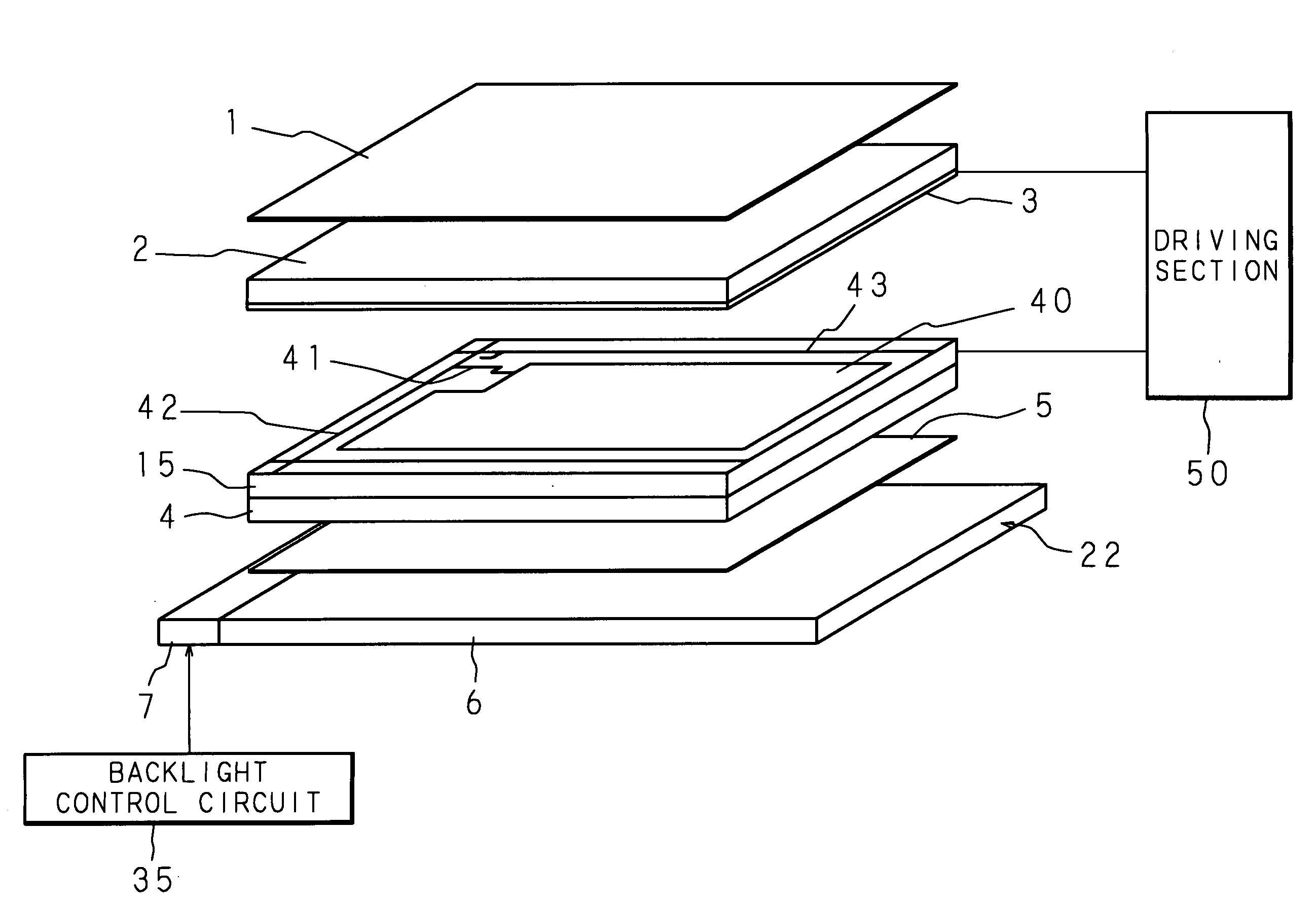
Figure 1 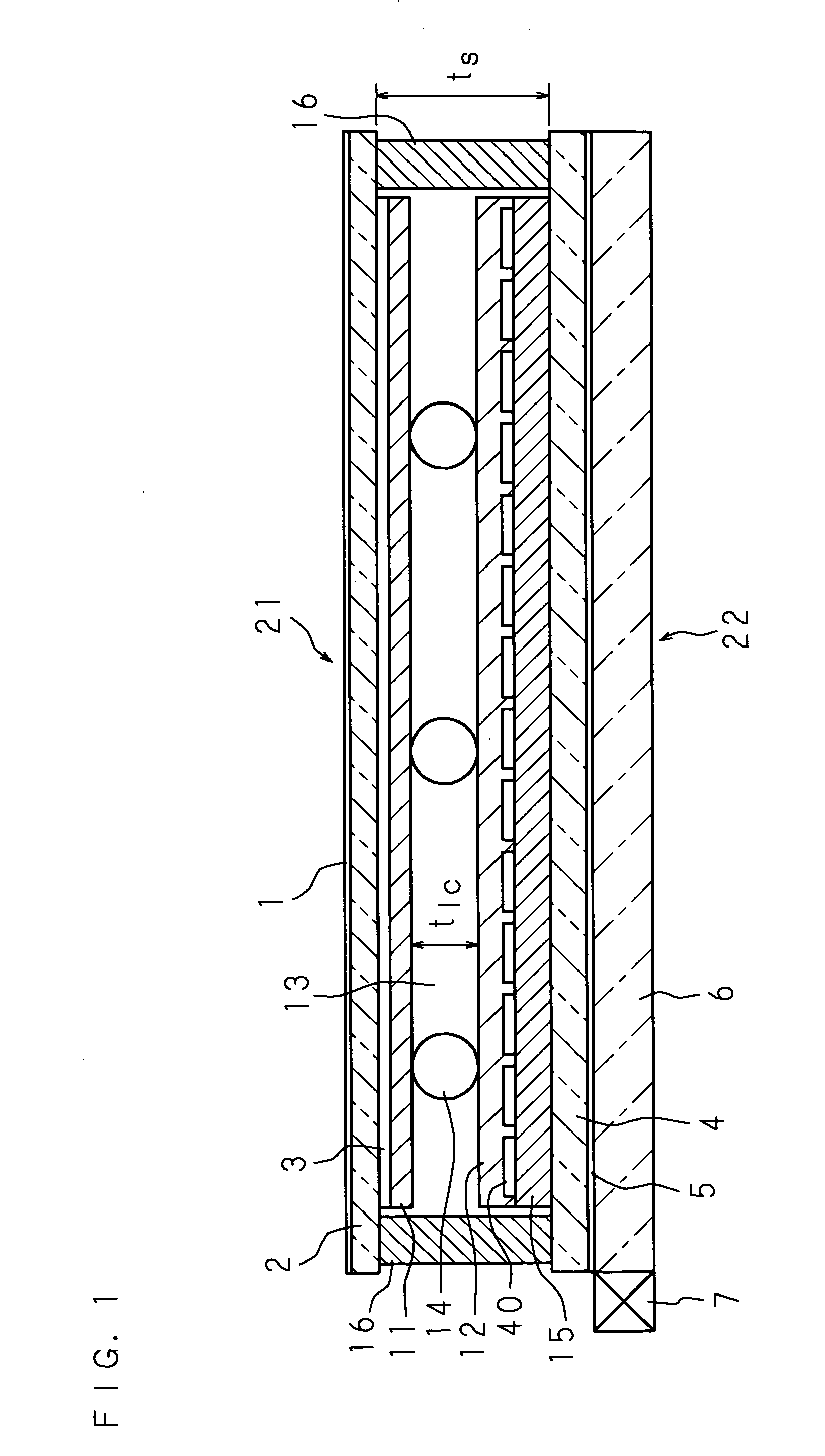
Figure 2 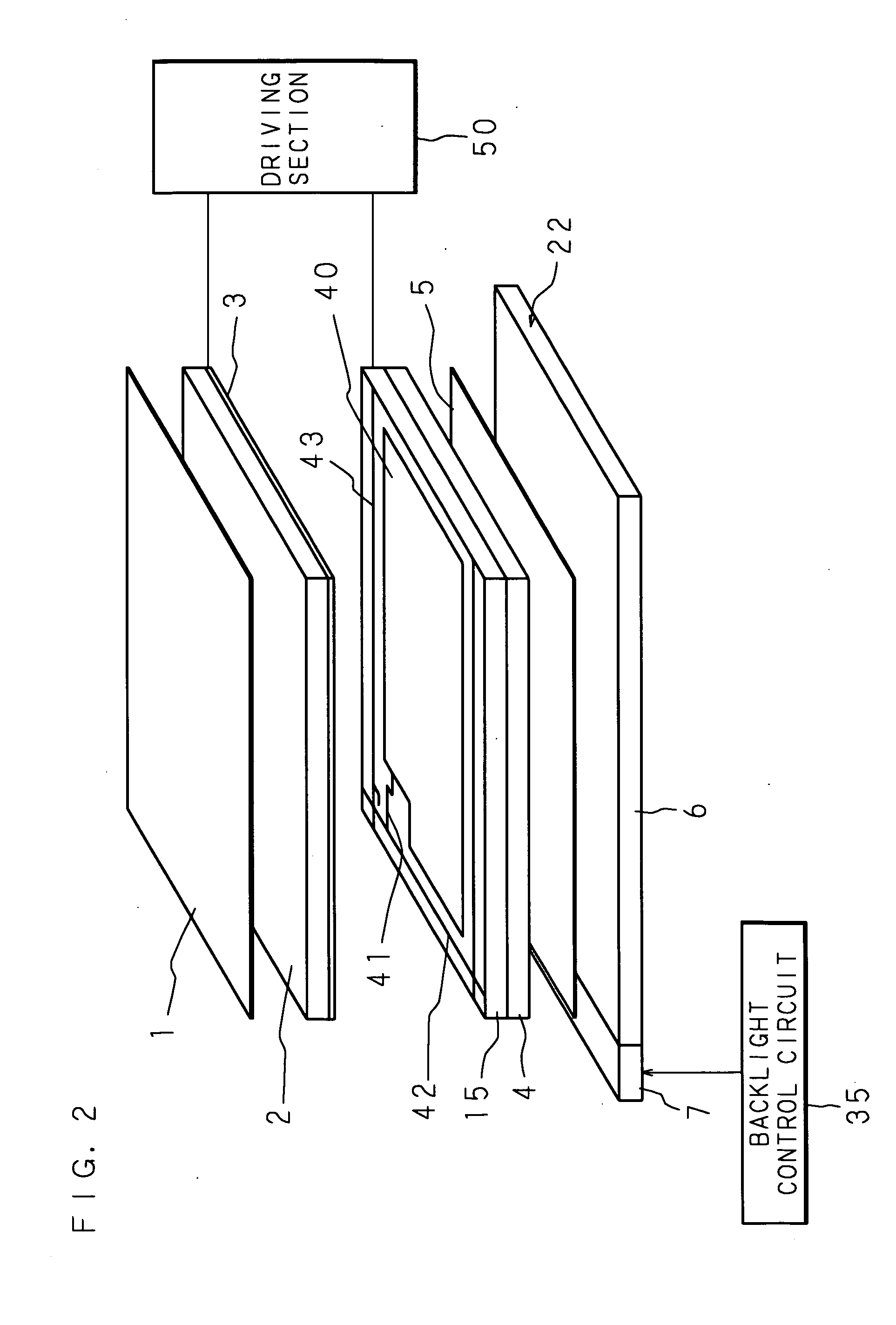
Figure 3
Abstract
Description
[0001] This application is Continuation Application under 35 U.S.C.§ 111(a) of PCT International Application No. PCT / JP2005 / 016649 which has an international filing date of Sep. 9, 2005 and designated the United State of America.BACKGROUND
[0002] 1. Technical Field
[0003] The present invention relates to a liquid crystal display device, and more particularly, concerns a liquid crystal display device in which a space formed by sealing a peripheral edge portion of a pair of opposing substrates by a sealing member is filled with a liquid crystal material.
[0004] 2. Description of Related Art
[0005] In recent years, together with developments of a so-called information society, electronic apparatuses, typically represented by personal computers, PDAs (Personal Digital Assistants) and the like, have been widely used. By the spread of these electronic apparatuses, there have been strong demands for portable apparatuses that can be used both in offices and outdoors, and small-size and light-weight ...
Examples
embodiment 1
[0032]FIG. 1 is a schematic cross-sectional view showing a liquid crystal panel and a backlight according to a first embodiment of a liquid crystal display device. FIG. 2 is a schematic view showing an example of the entire structure of the liquid crystal display device. FIG. 3 is a block diagram showing a circuit structure of the liquid crystal display device. FIG. 4 is a schematic view showing an example of a structure of an LED (Light Emitting Diode) array serving as a light source for the backlight.
[0033]Reference numerals 21 and 22 indicate a liquid crystal panel and a backlight whose cross-sectional structures are shown in FIG. 1. As shown in FIGS. 1 and 2, the backlight 22 is configured by an LED array 7 and a light directing and diffusing plate 6. As shown in FIGS. 1 and 2, the liquid crystal panel 21 has a structure in which a polarizer 1, a glass substrate 2, a common electrode 3, a glass substrate 4 and a polarizer 5 are stacked in this order from the upper layer (surface...
embodiment 2
[0046]FIG. 6 is a schematic cross-sectional view showing a liquid crystal panel and a backlight according to a second embodiment of a liquid crystal display device. In FIG. 6, those parts that are the same as those shown in FIG. 1 are indicated by the same reference numerals, and the description thereof is omitted.
[0047]In the second embodiment shown in FIG. 6, as well as a flat layer 15 on the glass substrate 4, a flat layer 17 is also placed between the glass substrate 2 and the common electrode 3. With this arrangement, the thickness of the sealing member 16 is adjusted. Thus, the liquid crystal panel of the present embodiment makes it possible to satisfy the relationship of ts / tlc≧2, more preferably, ts / tlc≧3.
[0048]In the liquid crystal display having the structure as shown in FIG. 6 also, the same display driving control as that of the aforementioned liquid crystal display device shown in FIG. 1 is of course carried out.
[0049]Although not shown in the Figures, only the flat lay...
example 1
[0053]A glass substrate 4 on which pixel electrodes 40, 40 . . . (number of pixels: 640×480, length across corners: 3.2 inches) were placed with a flat layer 15 made of an acrylic material with a thickness of 2 μm being interposed therebetween and a glass substrate 2 having a common electrode 3 were washed, and these were then coated with polyimide and baked at 200° C. for one hour so that polyimide films of about 200 Å were formed as alignment films 11 and 12. Moreover, these alignment films 11 and 12 were rubbed with a cloth made from rayon, and these two substrates were superposed one on the other, with the rubbing directions being made in parallel with each other, with a gap being maintained therein by using a sealing member 16 that is made from an epoxy resin and placed on a peripheral edge portion and spacers 14 made of silica having an average particle size of 1.6 μm; thus, empty panels with a gap maintained therein were manufactured.
[0054]A ferroelectric liquid crystal mater...