
High output resistance, wide swing charge pump
a charge pump and output resistance technology, applied in the field of charge pumps, can solve the problems of degrading system performance, degrading pll locking speed and jitter performance, etc., and achieves the effects of wide operation voltage range, increased output resistance, and increased output resistan
Patent Information
- Authority / Receiving Office
- US · United States
- Patent Type
- Applications(United States)
- Current Assignee / Owner
- Publication Date
- 2009-02-05
- Estimated Expiration
- Not applicable · inactive patent
Smart Images
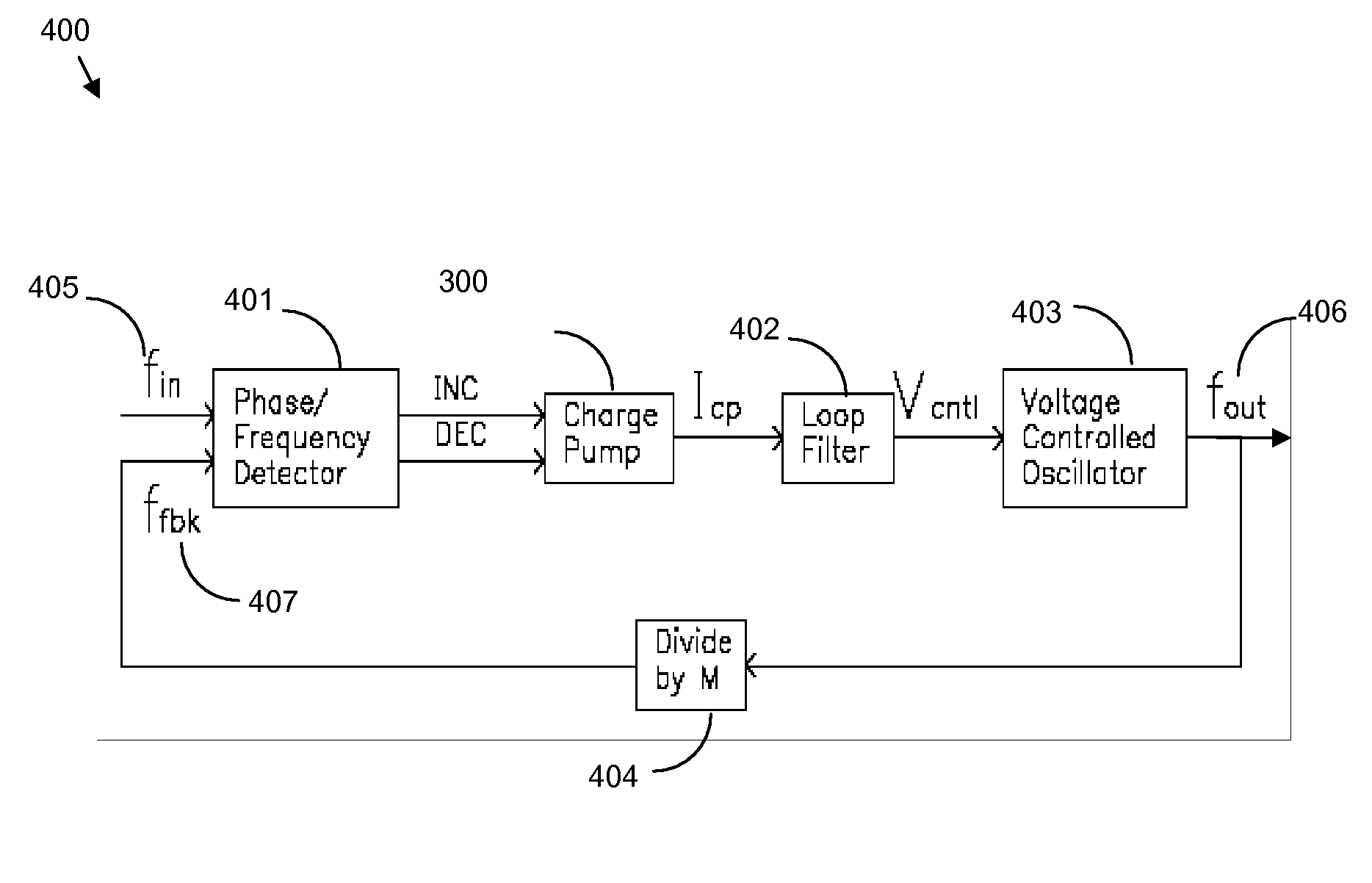
Figure 1 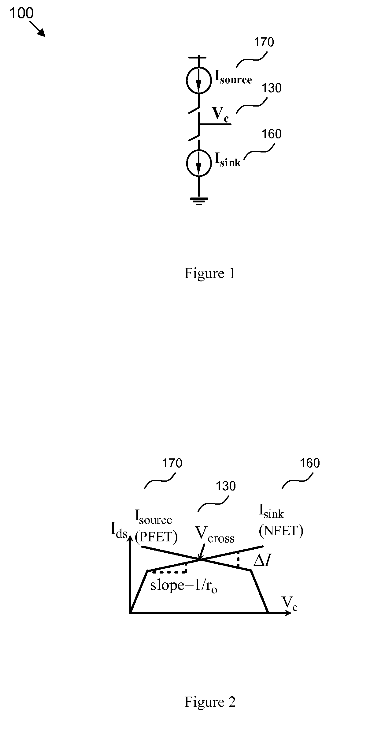
Figure 2 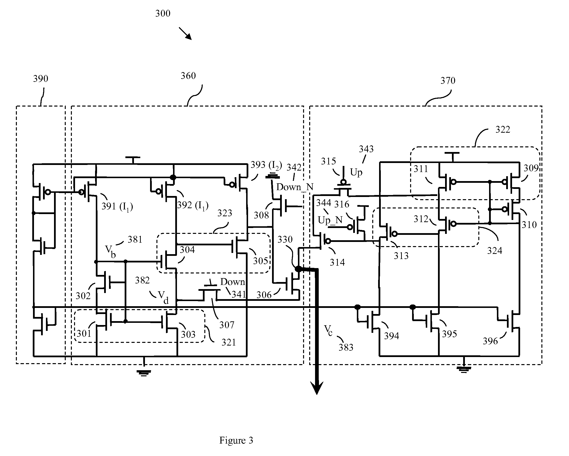
Figure 3
Abstract
Description
BACKGROUND
[0001] 1. Field of the Invention
[0002] The embodiments of the invention generally relate to charge pumps and, more particularly, to an improved charge pump structure having high output resistance and a wide swing.
[0003] 2. Description of the Related Art
[0004] The charge pump is an important circuit that is widely used in mixed signal systems. For example, in phase-locked loop circuits (PLL's), the charge pump is used to convert phase error detected by a phase / frequency detector (PFD) to analog voltage signals that are supplied to a voltage controlled oscillator. The charge pump consists of a charging current source and a discharging current sink. As a rule of thumb, it is important to ensure the current source and current sink have the same magnitude currents (e.g., in order to ensure optimal PLL performance). That is, large current mismatch between the components in the charge pump may degrade system performance, for instance, by introducing steady-state phase offset and incr...
Examples
Embodiment Construction
[0026]The embodiments of the invention and the various features and advantageous details thereof are explained more fully with reference to the non-limiting embodiments that are illustrated in the accompanying drawings and detailed in the following description. It should be noted that the features illustrated in the drawings are not necessarily drawn to scale. Descriptions of well-known components and processing techniques are omitted so as to not unnecessarily obscure the embodiments of the invention. The examples used herein are intended merely to facilitate an understanding of ways in which the embodiments of the invention may be practiced and to further enable those of skill in the art to practice the embodiments of the invention. Accordingly, the examples should not be construed as limiting the scope of the embodiments of the invention.
[0027]As mentioned above, the charge pump is an important circuit that is widely used in mixed signal systems, such as phase-locked loop (PLL) c...