
Magnetic Substance-Containing Insulator and Circuit Board and Electronic Device Using the Same
a technology of magnetic substance and insulator, which is applied in the direction of cross-talk/noise/interference reduction, coating, transportation and packaging, etc., can solve the problems of signal reflection and radiation in the line between elements, and the power consumption is large at the terminator terminating the line, so as to improve the characteristic impedance, increase the permeability, and reduce power consumption
Patent Information
- Authority / Receiving Office
- US · United States
- Patent Type
- Applications(United States)
- Current Assignee / Owner
- Publication Date
- 2009-05-14
- Estimated Expiration
- Not applicable · inactive patent
Smart Images
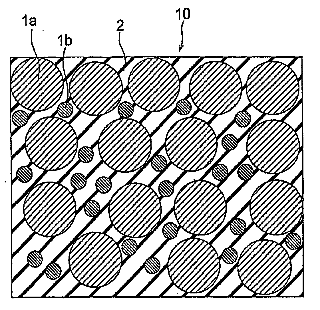
Figure 1 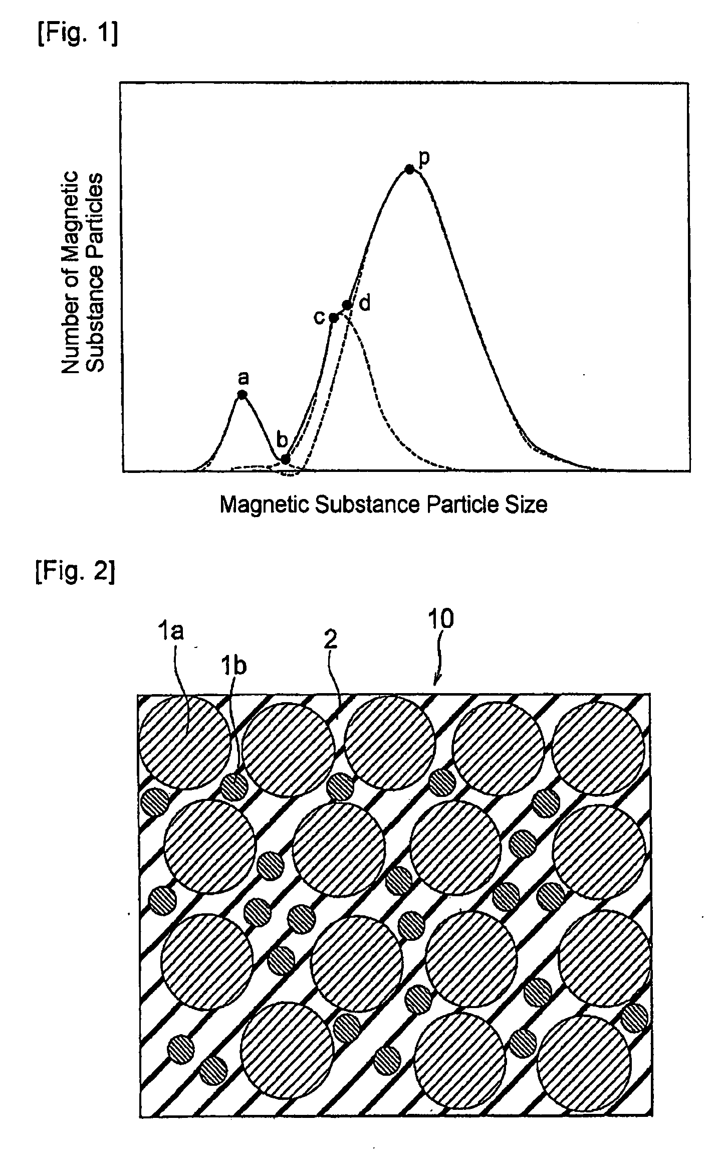
Figure 2 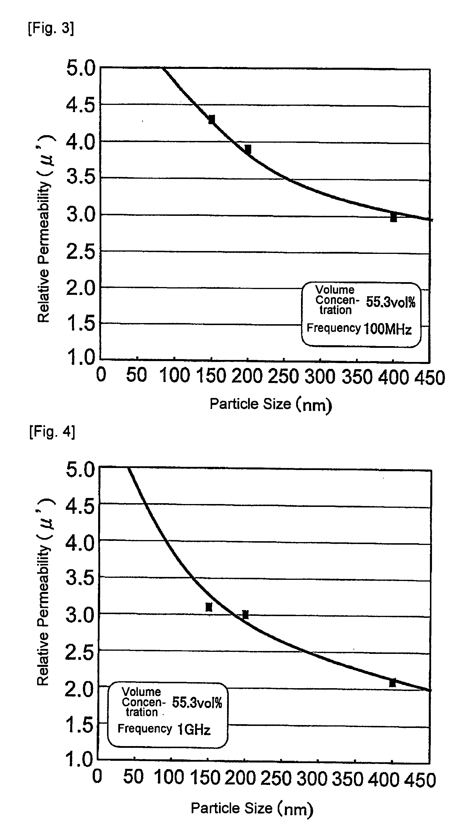
Figure 3
Abstract
Description
TECHNICAL FIELD
[0001] This invention relates to an insulator material and a circuit board for use, for example, as a high-frequency printed wiring board and, more specifically, relates to an insulating material and a circuit board enabling low power consumption, excellent in crosstalk and radiation noise suppression function, and capable of improving the quality of a signal propagating in a line.BACKGROUND ART
[0002] The signal rise rates have increased due to an improvement in operating speed of LSI, such as CPU, and thus a problem, such as signal reflection and radiation in a line between elements is becoming serious.
[0003] With respect to such a problem, wiring called a signal transmission line with controlled characteristic impedance is formed on a circuit board, thereby attempting to suppress signal reflection and crosstalk between elements.
[0004] On the other hand, use is generally made of a characteristic impedance of about several tens of Ω to 100Ω and there arises a problem that...
Examples
example 1
[0105]In Example 1 of this invention, an example of applying this invention to a circuit board will be described using FIG. 15. FIG. 15 is a sectional view showing the structure of a circuit board in Example 1 of this invention. Referring to FIG. 15, the circuit board includes a magnetic substance-containing insulator 10, plural metal lines 11, and a connecting portion 12 connecting these metal lines 10 together and was fabricated by the generally known build-up method.
[0106]The magnetic substance-containing insulator 10 in this circuit board 101 was fabricated in the following manner. First magnetic substance powder having an average particle size of 20 nm (ultrafine Fe powder manufactured by Shinku Yakin Co., Ltd.) and second magnetic substance powder having an average particle size of 200 nm (Ni powder manufactured by JFE Mineral Co., Ltd.) were mixed little by little into a dispersion solution in which a higher fatty acid ester as a surfactant was dissolved in a 4:3 mixed soluti...
example 2
[0113]In Example 2 of this invention, an example of applying this invention to an electronic component will be described using FIG. 17. FIG. 17 is a schematic diagram showing a chip inductor 105 as an electronic component according to an example of this invention. Referring to FIG. 17, the chip inductor 105 comprises a magnetic substance-containing insulator board 3 and an inductance line 4. The inductance line 4 was obtained by laminating a copper foil with a thickness of 20 μm on the magnetic substance-containing insulator board 3 and patterning the copper foil by the photolithography method. The line width was set to 100 μm and the line was in the form of a square coil with one turn. A magnetic substance-containing insulator board 5 being the same as the magnetic substance-containing insulator board 3 was attached onto the coil under pressure by the pressing method and cutting was performed into 1.5 mm square to extract electrodes, thereby obtaining the chip inductor.
[0114]The ma...