

photodiode
a photodiode and photodiode technology, applied in the field of photodiodes, can solve the problems of long travel distance of holes, difficult to satisfy the demands of difficulty in sufficiently alleviating the trade-off between increased sensitivity and speed, so as to achieve high-speed response, small width, and large specific resistance
Patent Information
- Authority / Receiving Office
- US · United States
- Patent Type
- Applications(United States)
- Current Assignee / Owner
- Publication Date
- 2009-06-11
Smart Images
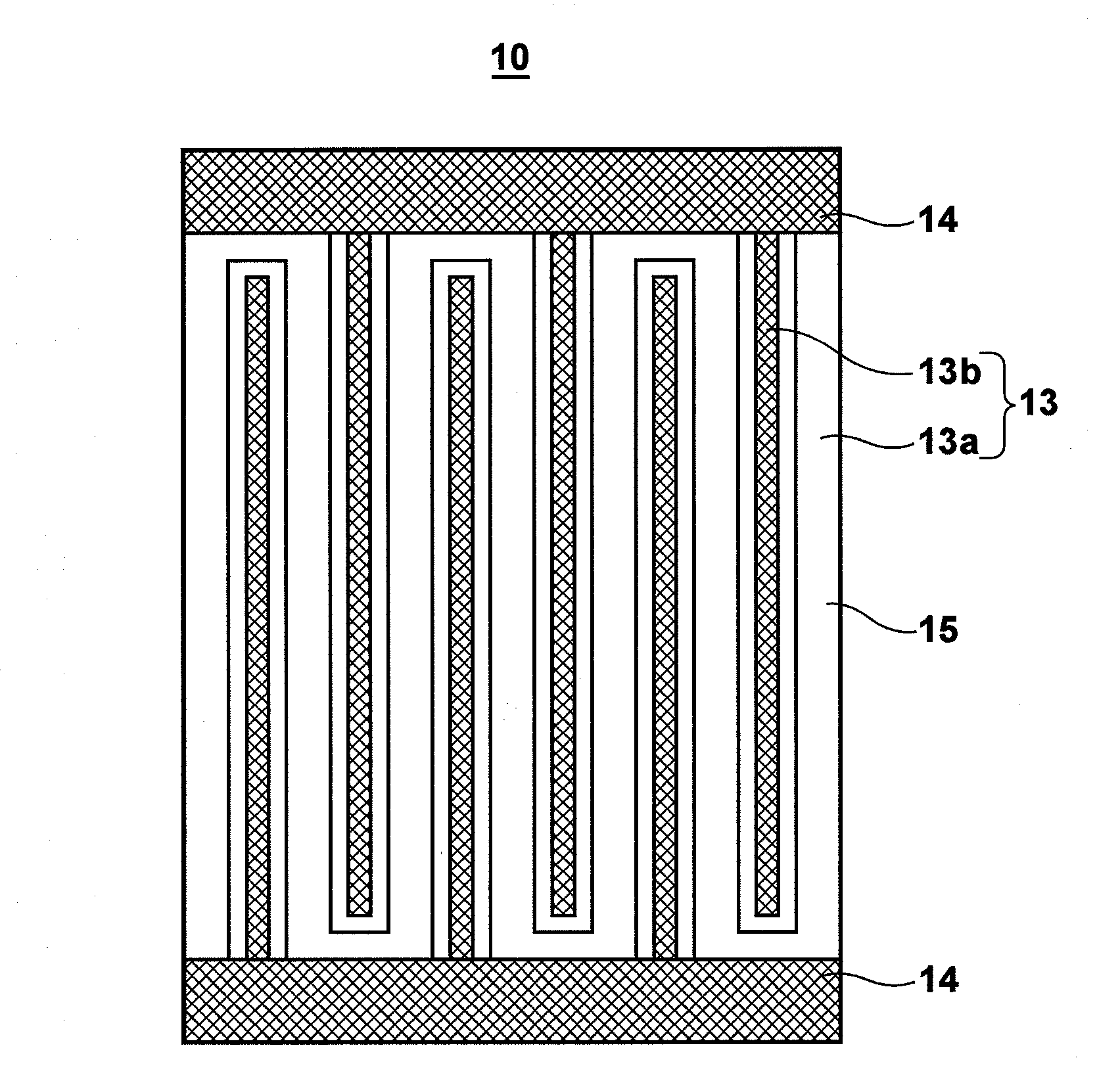
Figure 1 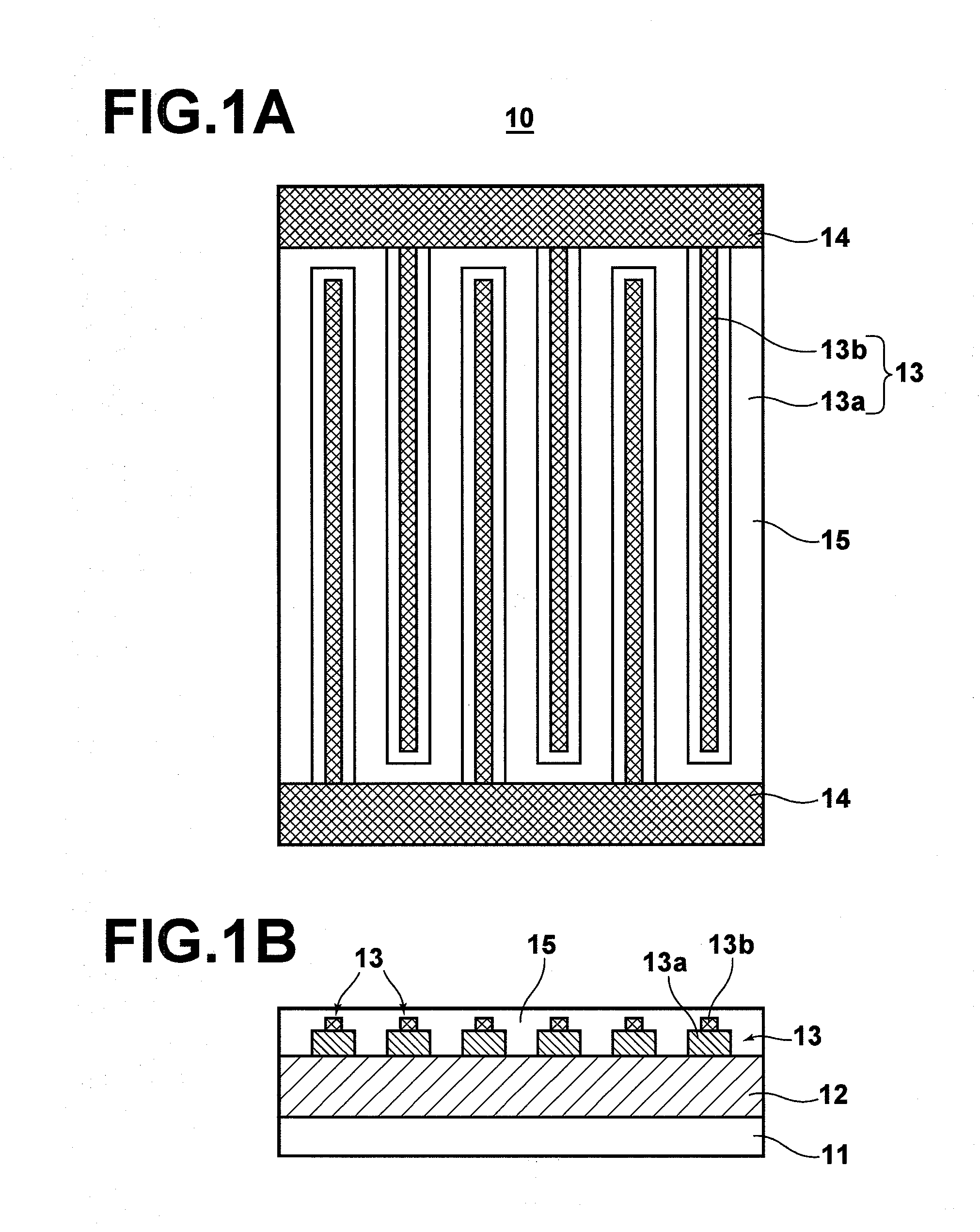
Figure 2 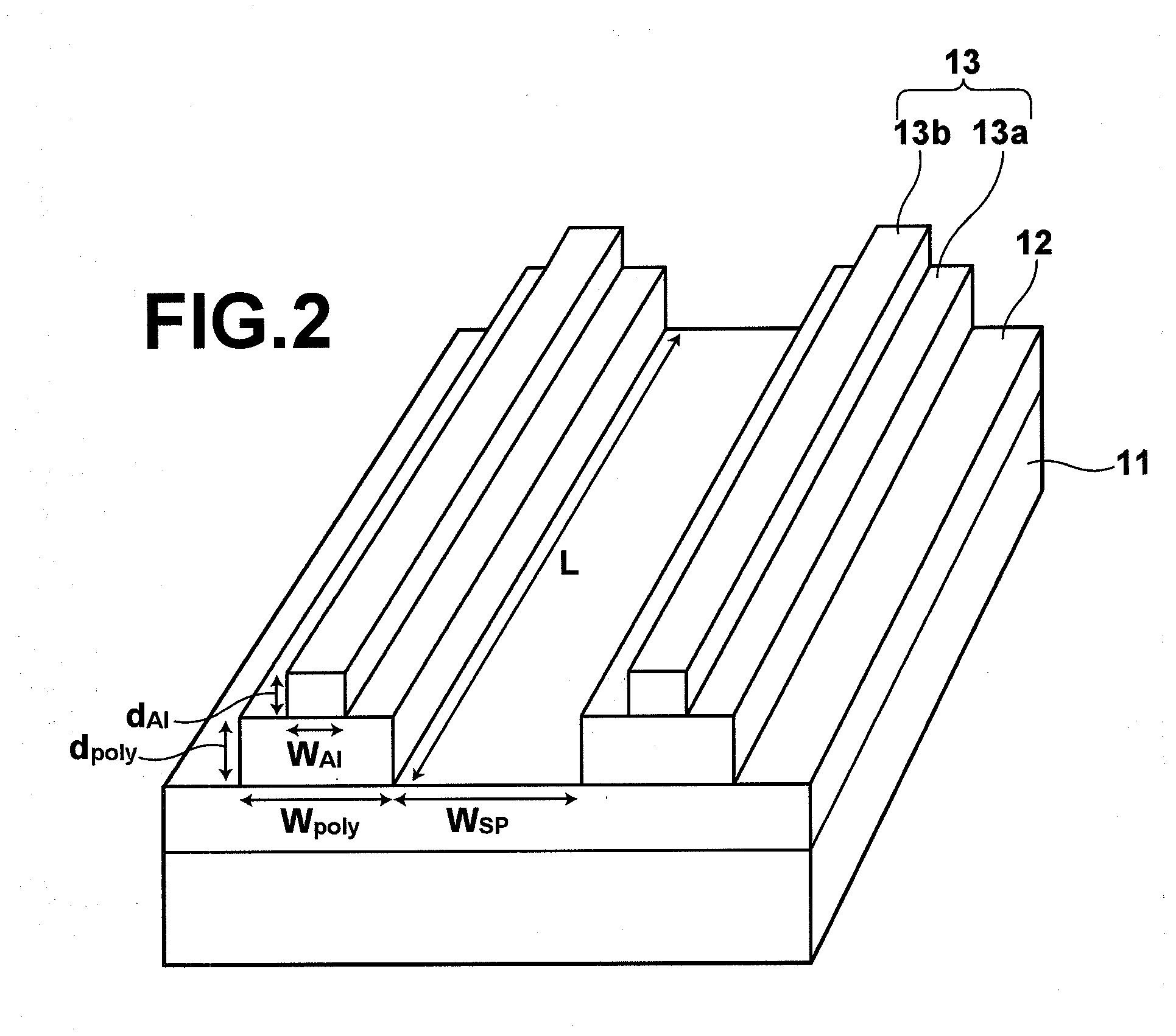
Figure 3
Abstract
Description
BACKGROUND OF THE INVENTION
[0001] 1. Field of the Invention
[0002] The present invention relates to a photodiode, and a method for manufacturing the same.
[0003] 2. Description of the Related Art
[0004] Recently, in order to cope with a dramatic increase in the capacity of networks, epitomized by the widespread use of the Internet, development of high-speed optical transmission systems has been sought. Today, optical fibers having comparatively large apertures that facilitate alignment, such as plastic optical fibers, multimode glass optical fibers, and the like, are drawing increased attention as optical fibers for use not with trunk line systems but “last one mile” transmission systems, including subscriber line systems. As optical receivers suitable for high speed and large aperture optical fibers, MSM (metal-semiconductor-metal) photodiodes, lateral PIN photodiodes, and the like, in which electrodes are arranged laterally, i.e., in the direction parallel to the surface of the substrate...
Examples
Embodiment Construction
[0034]Hereinafter, an exemplary embodiment of the present invention will be described in detail with reference to the accompanying drawings. FIGS. 1A and 1B respectively illustrate a schematic planar shape and a schematic sectional elevational shape of the photodiode 10 according to an embodiment of the present invention. The photodiode of the present embodiment is, as an example, a MSM (metal-semiconductor-metal) lateral photodiode. As illustrated, the photodiode 10 includes: a semiconductor substrate 11; an active layer 12 formed on the substrate 11; a comb electrode including a plurality of comb electrode fingers 13 arranged side by side on the active layer 12 with appropriate spacing; electrodes 14 connected to the comb electrode fingers 13; and a passivation layer 15 formed on the comb electrode fingers 13.
[0035]In FIG. 1A, the upper electrode 14 is the positive electrode and connected to a signal line, and lower electrode 14 is the negative electrode and grounded. Thus, the co...