
Light guides
Patent Information
- Authority / Receiving Office
- US · United States
- Current Assignee / Owner
- Publication Date
- 2010-11-25
Smart Images
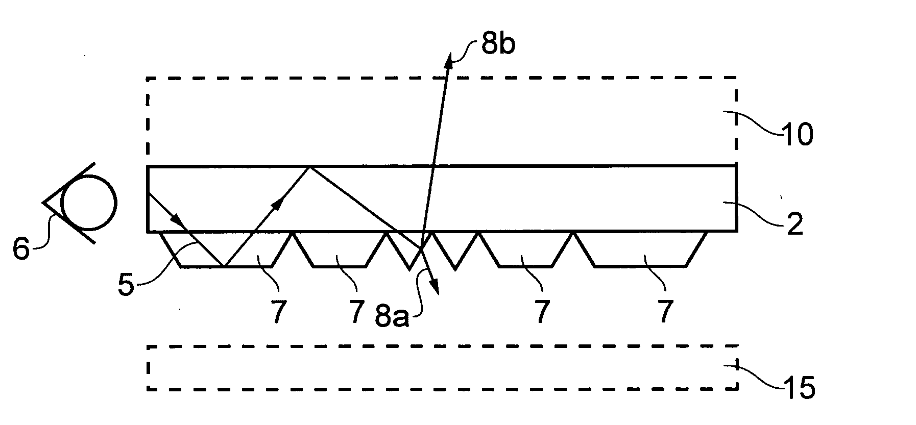
Figure 1 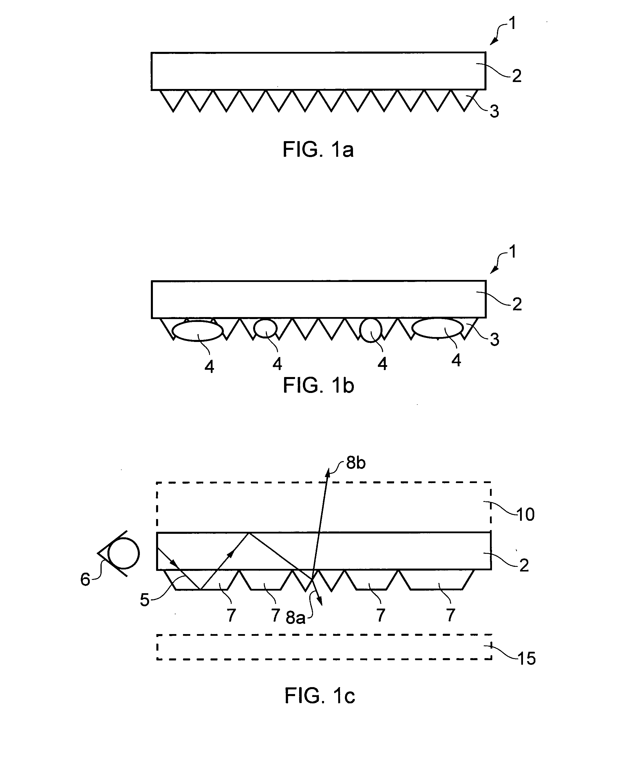
Figure 2 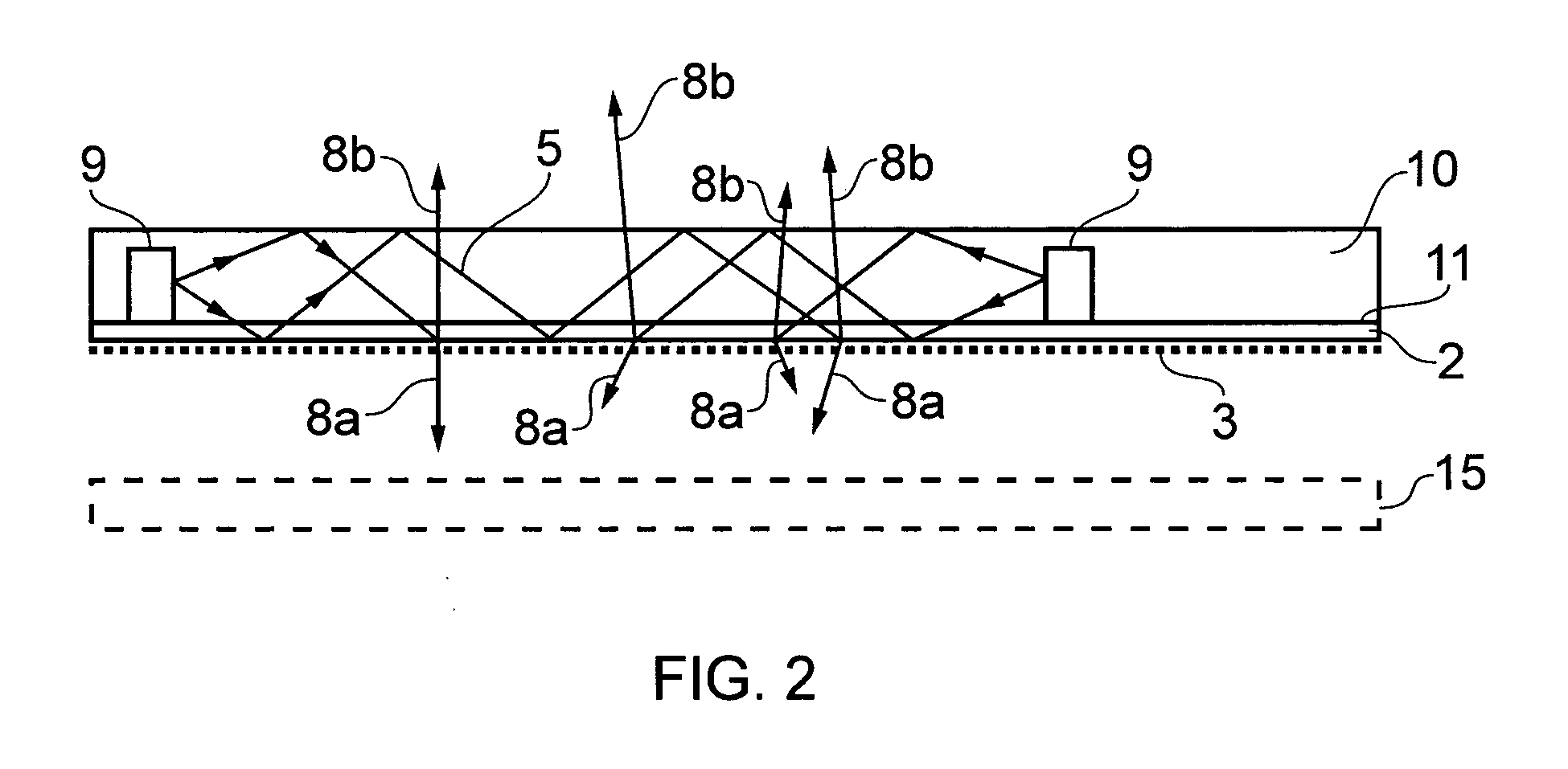
Figure 3
Abstract
Description
FIELD OF THE INVENTION
[0001] This invention relates to film layer which is suitable for use in a light guide plate and methods of forming said film layer and light guide plate. The invention also relates to the light guide plate and light guide devices made therefrom. The film and light guide plate are suitable for use in a range of applications, particularly in connection with the backlighting of displays, for example, liquid crystal displays.BACKGROUND OF THE INVENTION
[0002] A number of routes and manufacturing processes exist for making light guide layers suitable for use in backlighting applications. Typically, a transparent polymer is injection moulded to form a thin plate with suitable surface features. The surface features disturb the total internal reflection of the light thus allowing light, guided inside the plate, to escape in a controlled manner.
[0003] However, there are a number of problems associated with such a technique, not least the expense associated with forming a s...
Examples
example 1
[0061]A light guide device was made as follows and with reference to FIG. 3 described above. 3M BEF III (Matte) was obtained from 3M and used as the film layer. Silver flake loaded solvent based polymer ink, which is a conducting ink, was screen printed onto the top side (non-microstructured side) of the BEF substrate. Windotex Gloss, an acrylic based, transparent UV curing polymer screen printable ink which is commercially available from MacDermid Autotype was printed on the reverse side of the substrate in a pattern to modify the BEF microstructure and provide the light scattering feature for uniform light output. In this example, the pattern was a series of small lines which were pitched across the surface at the 1000 micron scale and sized at the 500 to 1000 micron scale near the LEDs and sized at the 100 to 500 micron scale towards the middle of the microstructured film, and further away from the LEDs, resulting in minimal planarising of the microstructure. This arrangement res...
example 2
[0063]A number of experiments were undertaken to test the use of specular reflective ink in combination with the microstructured film used in Example 1. A pattern of mirrored prisms were deposited on the microstructures. By using a commercially available chrome, air drying ink, the acrylic microstructure / ink interface was made reflective from the acrylic side. The reflective ink was printed at 100 Dots Per Inch (DPI).