
Method for manufacturing semiconductor device
Patent Information
- Authority / Receiving Office
- US · United States
- Current Assignee / Owner
- Publication Date
- 2012-07-05
Smart Images
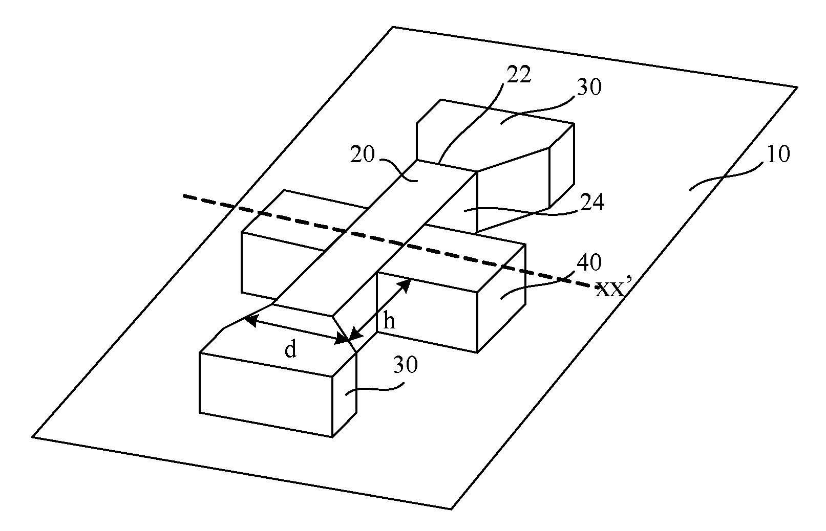
Figure 1 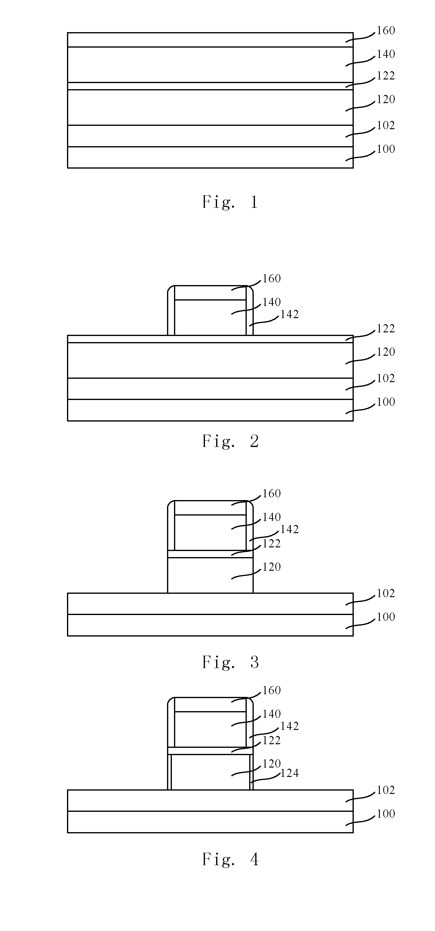
Figure 2 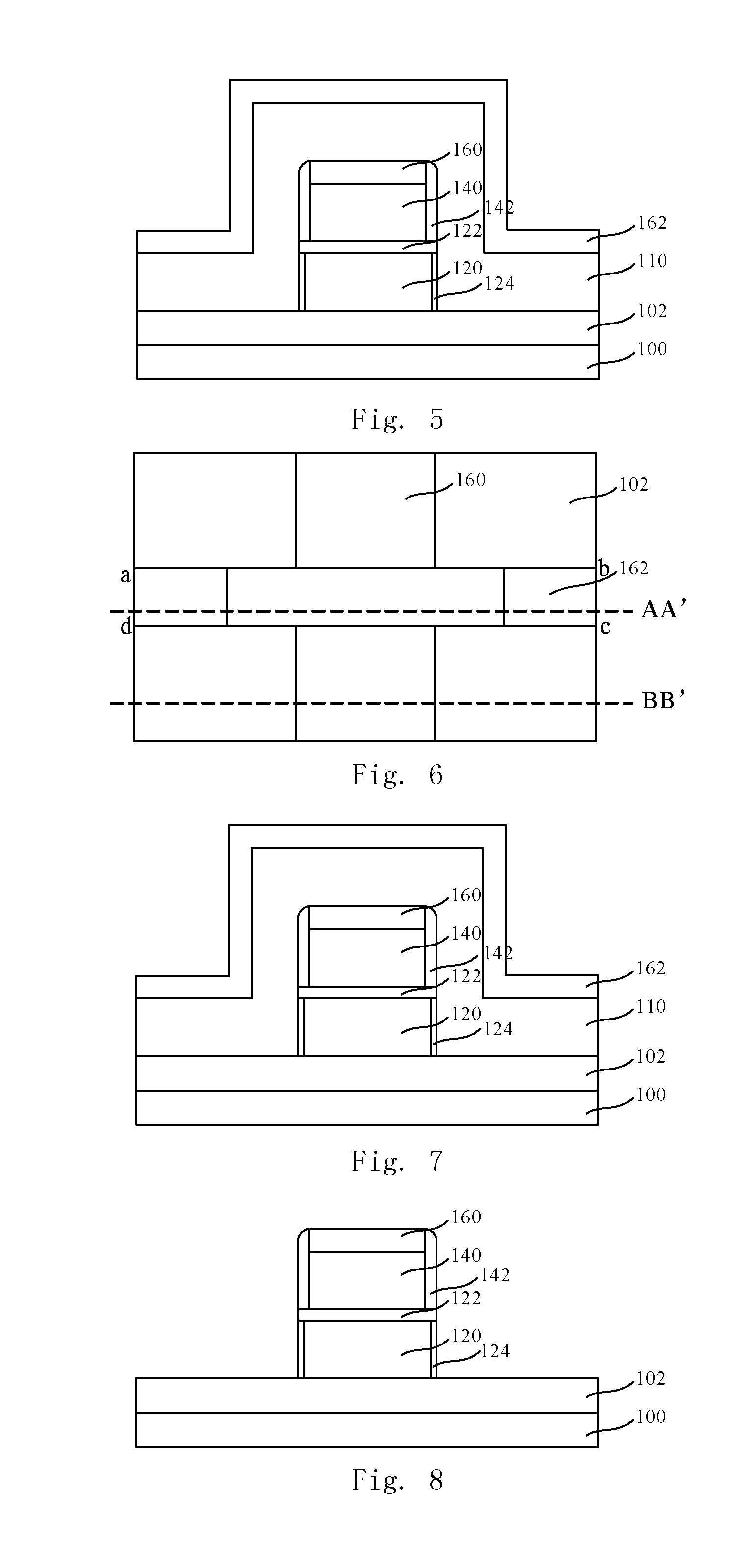
Figure 3
Abstract
Description
FIELD OF THE INVENTION
[0001] The present invention relates to semiconductor technology, and particularly, to a method for manufacturing a semiconductor device.BACKGROUND OF THE INVENTION
[0002] When the channel length of a metal oxide semiconductor field effect transistor (MOSFET) becomes smaller continuously, many negligible effects in the long-channel model of the MOSFET becomes more significant, and has even been a dominant factor determining its properties. These effects are commonly referred to as short channel effects. The short channel effect deteriorates electrical properties of the device, which, for example, leads to a reduced gate threshold voltage, increased power consumption, and a lowered signal-to-noise ratio.
[0003] To suppress the short channel effect, the channel has to be doped with more elements such as phosphorus, boron, and the like, which, however, decreases the carrier mobility in the channel of the device. Moreover, it is difficult to provide a steep doping profi...
Examples
Embodiment Construction
[0044]The disclosure below provides various embodiments or examples for carrying out the technical solution of the present invention. Although the components and arrangements of some specific examples are described, they are only examples, and are not construed as limiting the present invention.
[0045]Moreover, reference numerals and / or letters are repeated in various embodiments. The repetition is for simplicity and clarity, and does not represent relationship between various embodiments and / or settings to be discussed below.
[0046]Various specific processes and / or materials are used in the present invention. Nevertheless, one skilled person in the art will appreciate that other processes and / or materials can also be used as alternatives without departing from the protection scope of the invention. It should be noted that boundaries of various regions described herein include necessary extensions introduced by the process.
[0047]According to the present invention, there is provided a ...