
Non-volatile memory device and manufacturing method thereof
a memory device and non-volatile technology, applied in the field of semiconductor devices, can solve the problems of no conductive vias are disposed under the dummy memory cells, and affecting the performance of the devi
Patent Information
- Authority / Receiving Office
- US · United States
- Patent Type
- Applications(United States)
- Current Assignee / Owner
- Publication Date
- 2022-11-17
Smart Images
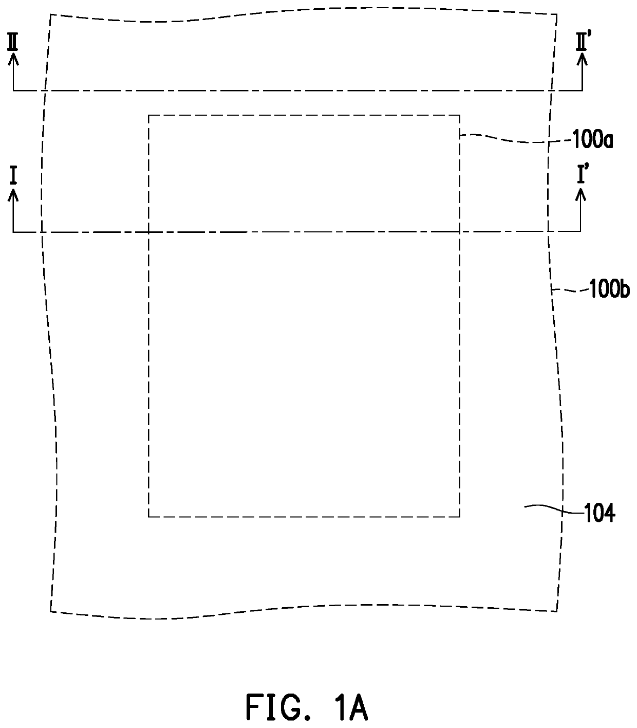
Figure 1 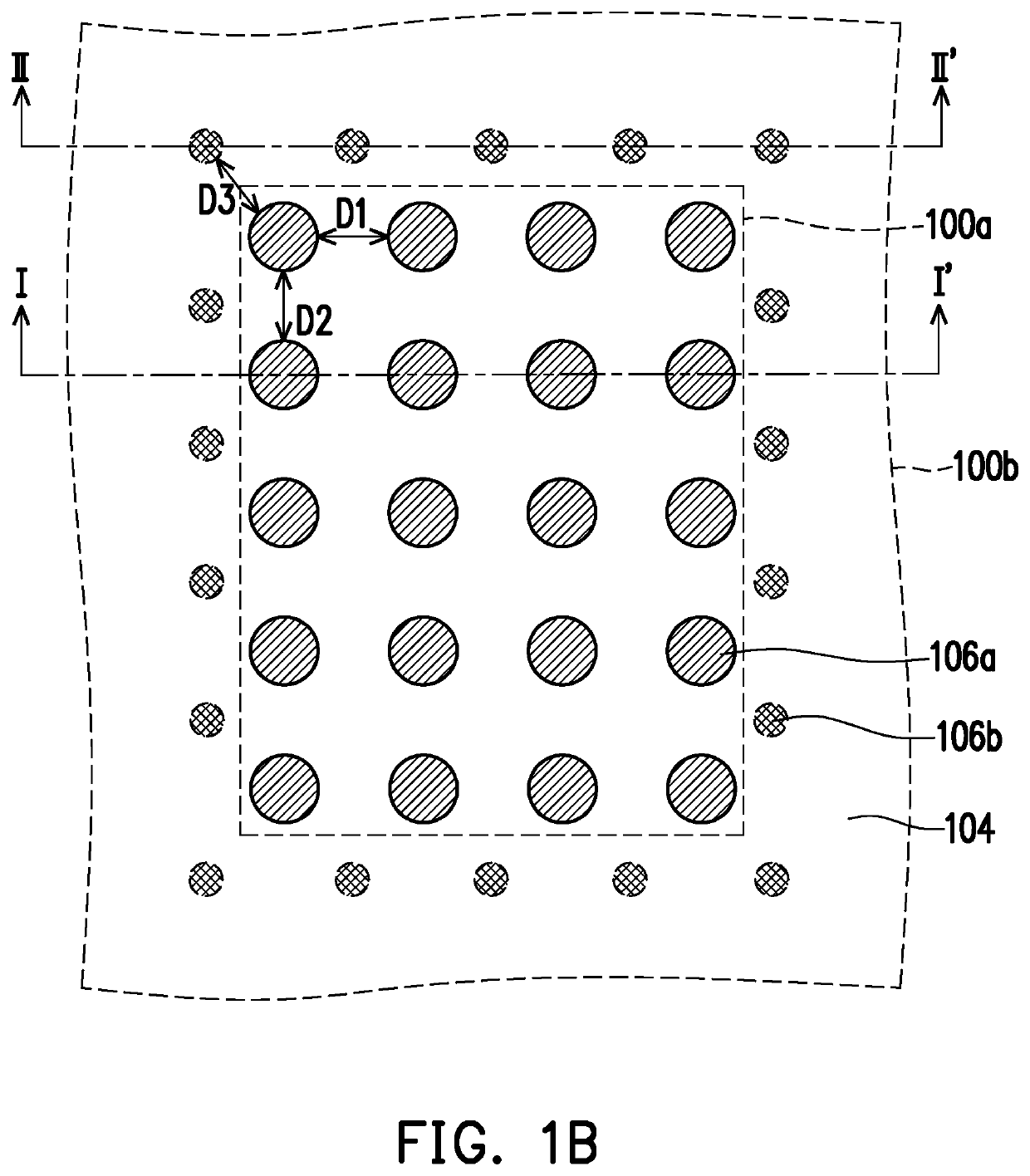
Figure 2 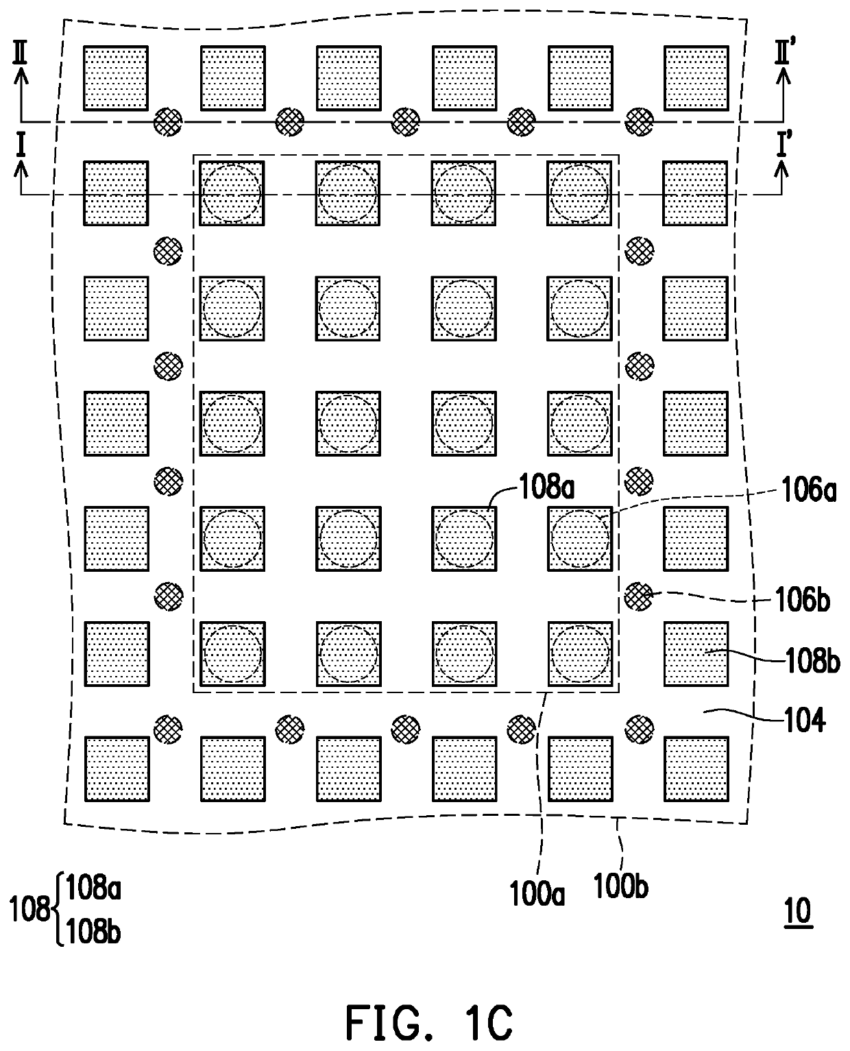
Figure 3
Abstract
Description
CROSS-REFERENCE TO RELATED APPLICATION
[0001] This application claims the priority benefit of China application serial no. 202110532868.6, filed on May 17, 2021. The entirety of the above-mentioned patent application is hereby incorporated by reference herein and made a part of this specification.BACKGROUNDTechnical Field
[0002] The present invention relates to a semiconductor device and a manufacturing method thereof, and particularly relates to a non-volatile memory device and a manufacturing method thereof.Description of Related Art
[0003] In the general magnetoresistive random access memory (MRAM) process, during the patterning process for forming memory cells, the optical effect may affect the profile of the memory cells located at the edge of the memory region, making the dimension of the memory cells located at the edge of the memory region smaller than the dimensions of other memory cells.
[0004] In order to avoid the above problem, currently a dummy region may be disposed around th...
Examples
Embodiment Construction
[0036]The embodiments are described in detail below with reference to the accompanying drawings, but the embodiments are not intended to limit the scope of the present invention. In addition, the drawings are for illustrative purposes only and are not drawn to the original dimensions. For the sake of easy understanding, the same elements in the following description will be denoted by the same reference numerals.
[0037]In the text, the terms mentioned in the text, such as “comprising”, “including”, “containing” and “having” are all open-ended terms, i.e., meaning “including but not limited to”.
[0038]When using terms such as “first” and “second” to describe elements, it is only used to distinguish the elements from each other, and does not limit the order or importance of the devices. Therefore, in some cases, the first element may also be called the second element, the second element may also be called the first element, and this is not beyond the scope of the present invention.
[0039...