
Wafer level creation of multiple optical elements
Patent Information
- Authority / Receiving Office
- US · United States
- Current Assignee / Owner
- Publication Date
- 2005-01-18
- Estimated Expiration
- Not applicable · inactive patent
Smart Images
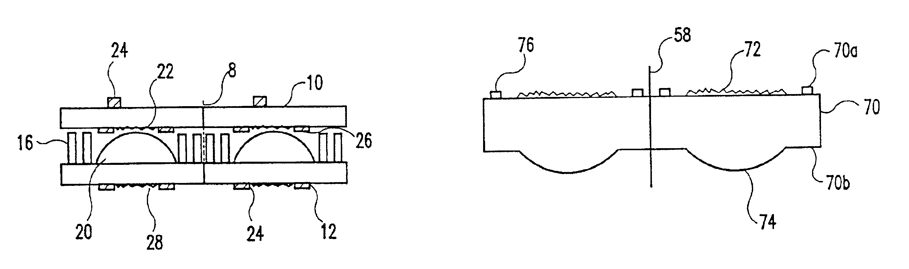
Figure 1 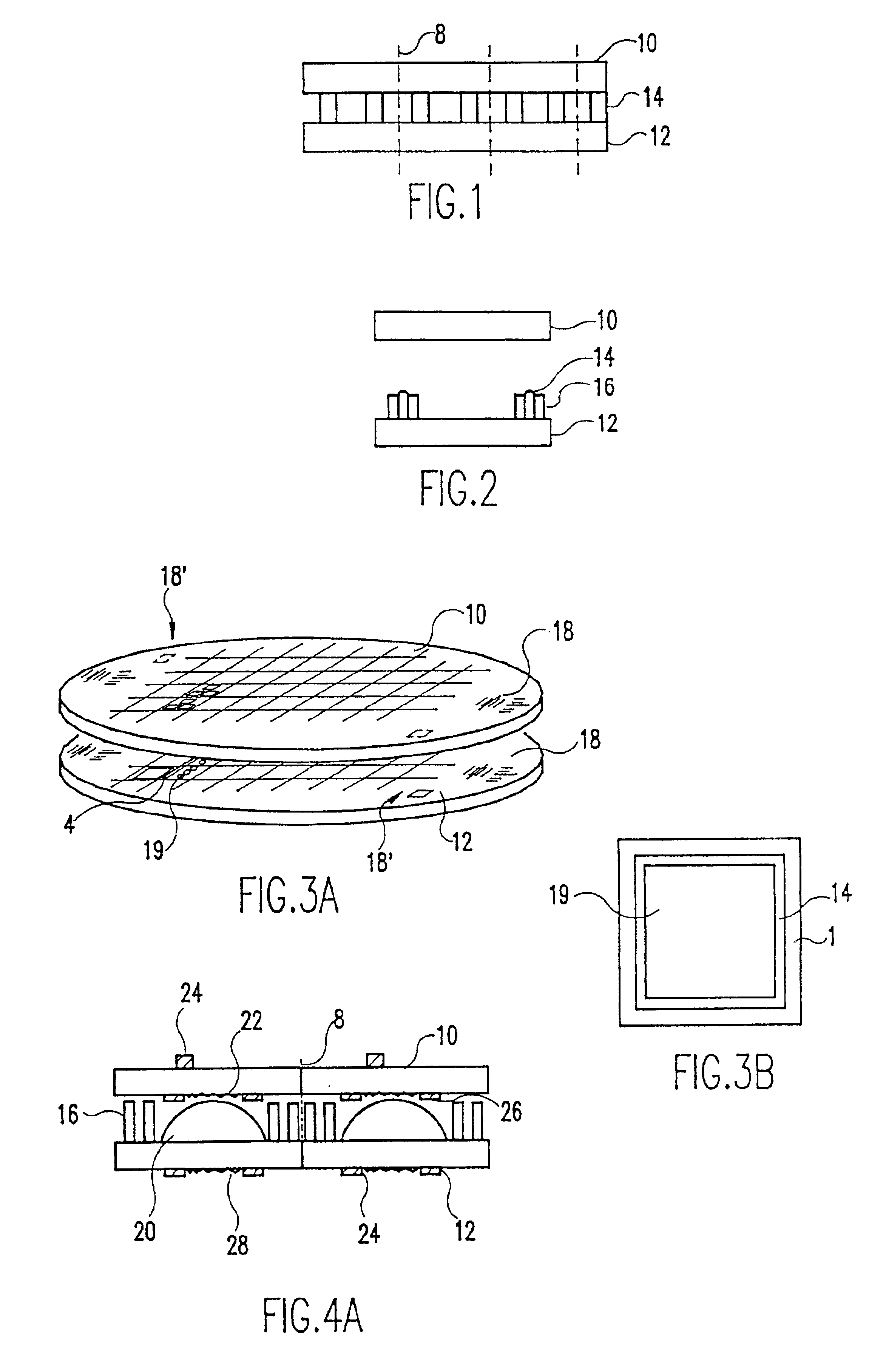
Figure 2 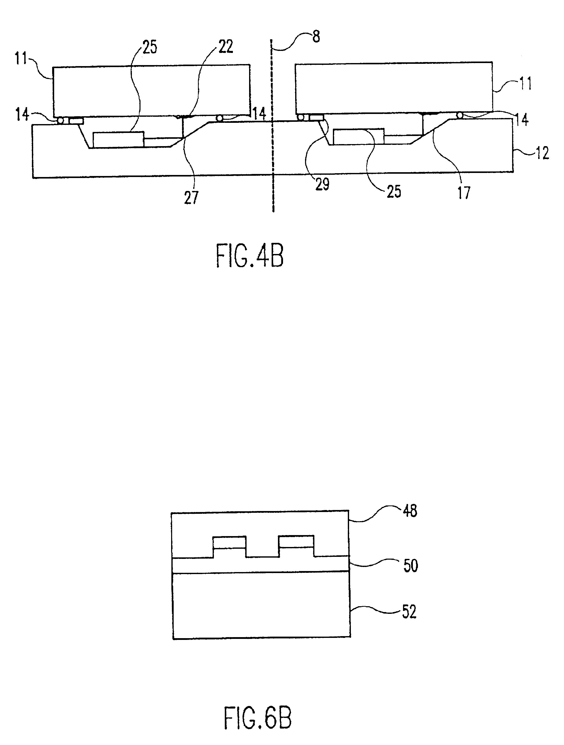
Figure 3
Abstract
Description
FIELD OF THE INVENTIONThe present invention is directed to integrating multiple optical elements on a wafer level. In particular, the present invention is directed to efficient creation of integrated multiple elements.BACKGROUND OF THE INVENTIONAs the demand for smaller optical components to be used in a wider variety of applications increases, the ability to efficiently produce such optical elements also increases. In forming such integrated multiple optical elements at a mass production level, the need for accurate alignment increases. Further, such alignment is critical when integrating more than one optical element.Integrated multiple optical elements are multiple optical elements stacked together along the z-axis, i.e., the direction of the light propagation. Thus, light travelling along the z-axis passes through the multiple elements sequentially. These elements are integrated such that further alignment of the elements with themselves is not needed, leaving only the integrate...
Examples
Embodiment Construction
As can be seen in FIG. 1, a first substrate wafer 10 and a second substrate wafer 12 are to be bonded together in order to provide integrated multiple optical elements. A wafer is a disc, typically 4, 6, 8, or 12 inches in diameter and typically having a thickness between 400 microns and 6 mm.
These wafers have an array of respective optical elements formed thereon on either one or both surfaces thereof. The individual optical elements may be either diffractive, refractive or a hybrid thereof. Dashed lines 8 indicate where the dicing is to occur on the wafers to provide the individual integrated elements.
A bonding material 14 is placed at strategic locations on either substrate in order to facilitate the attachment thereof. By surrounding the optical elements which are to form the final integrated die, the adhesive 14 forms a seal between the wafers at these critical junctions. During dicing, the seal prevents dicing slurry from entering between the elements, which would result in co...