
Method and apparatus for providing lens aberration compensation by illumination source optimization
a technology of illumination source and compensation method, applied in the field of photolithography, can solve the problems of reducing the size of an integrated circuit, reducing cd (critical dimension) of the corresponding mask pattern approaching the resolution limit of the optical exposure tool, so as to prolong the useful life of the projection lens, improve imaging performance, and improve pattern fidelity
Patent Information
- Authority / Receiving Office
- US · United States
- Patent Type
- Patents(United States)
- Current Assignee / Owner
- Publication Date
- 2006-04-25
Smart Images
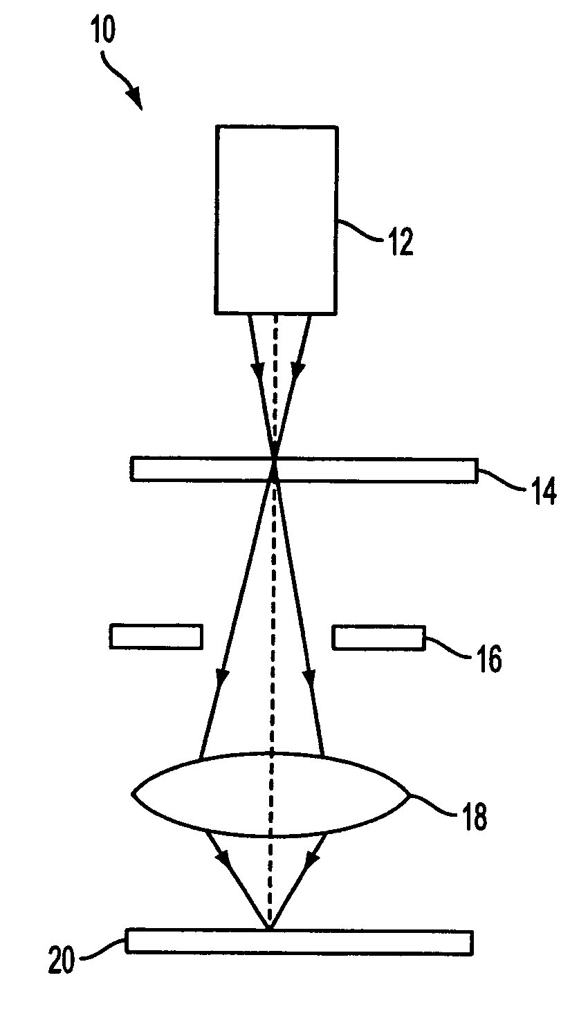
Figure 1 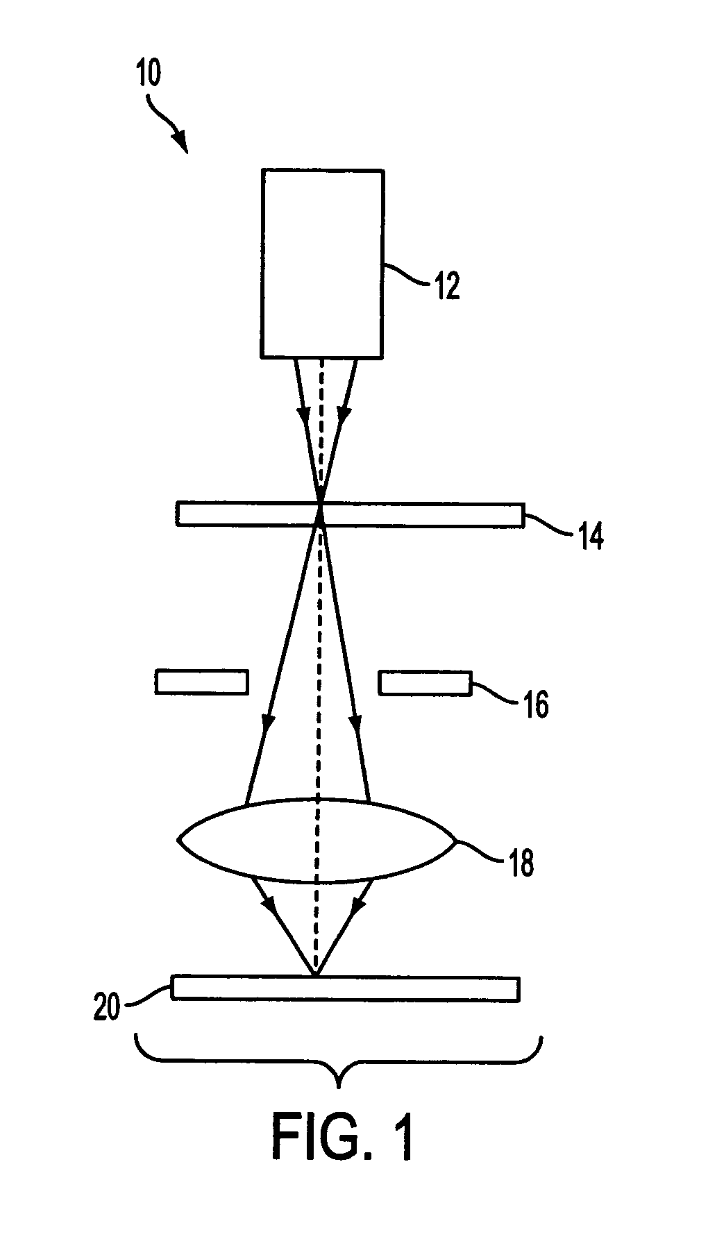
Figure 2 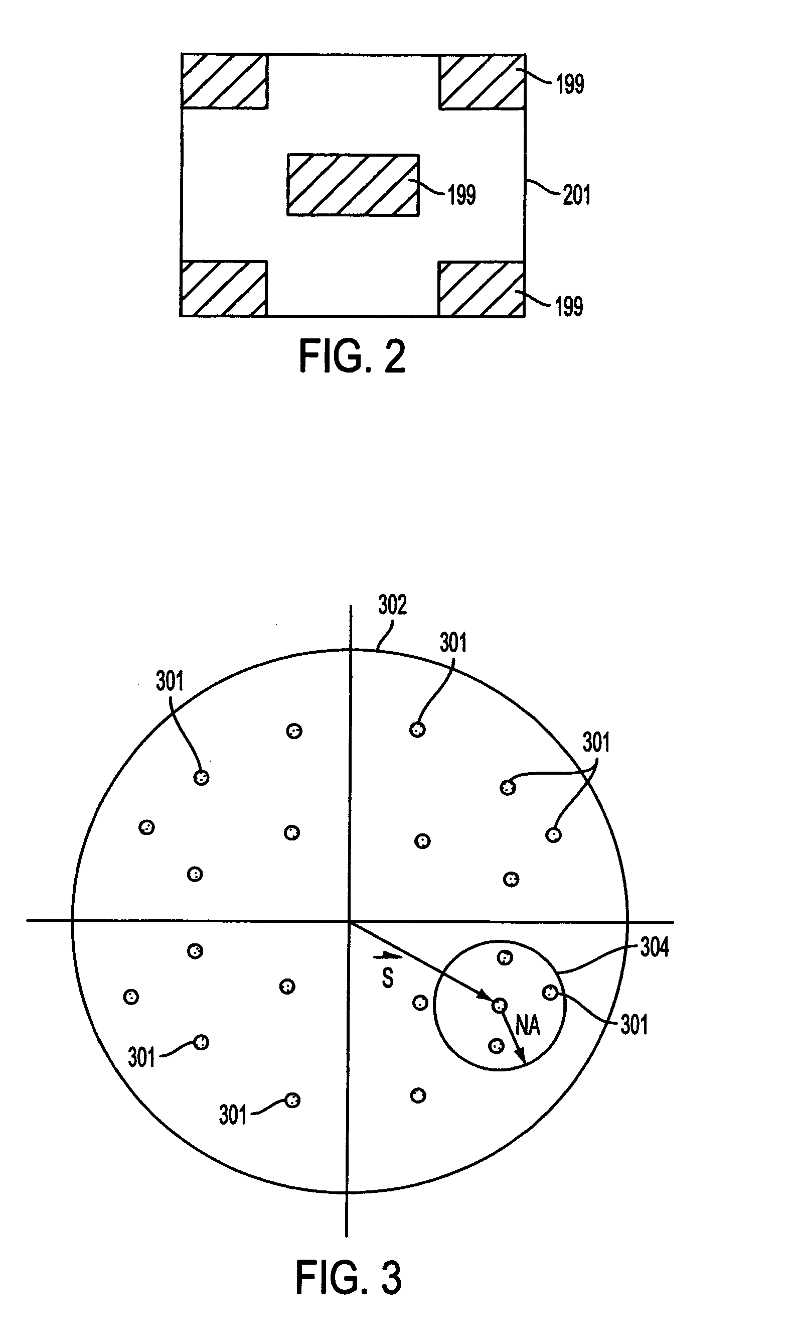
Figure 3
Abstract
Description
[0001] This application claims the benefit of 60 / 425,309, filed Nov. 12, 2002.FIELD OF THE INVENTION
[0002] The present invention relates to photolithography, and in particular relates to a method for providing improved performance of lithographic processes by compensating for lens aberrations by performing an illumination source optimization process. In addition, the present invention relates to a device manufacturing method which incorporates the optimization process and utilizes a lithographic apparatus comprising a radiation system for providing a projection beam of radiation; a mask table for holding a mask, serving to pattern the projection beam; a substrate table for holding a substrate; and a projection system for projecting the patterned projection beam onto a target portion of the substrate.BACKGROUND OF THE INVENTION
[0003] Lithographic projection apparatus (tools) can be used, for example, in the manufacture of integrated circuits (ICs). In such a case, the mask contains a ci...
Examples
Embodiment Construction
[0033]As explained in further detail below, the object of the lithographic optimization process of the present invention is to first define and then minimize a cost metric “C” under a varying set of imaging conditions, where the cost metric C is a function of a set of process parameters which returns a numeric value that quantifies the performance of the imaging system. Importantly, the cost metric C must reflect the effects of lens aberration on imaging perform. In accordance with the present invention, the cost metric quantifies the effect of the shape of the illumination source on the resulting image printed on the substrate. The smaller the cost metric, the better the imaging process will perform (i.e., the more accurately the resulting image matches the target pattern).
[0034]As a practical matter, lithographic process optimization involves satisfying multiple constraints. Examples of such constraints include, but are not limited to, maximizing the image log slope, maximizing th...