
Scanner system
a scanning system and scanning beam technology, applied in the field of scanning surfaces, can solve the problems of uniform power of the long-distance beam of the oblong beam, and achieve the effects of reducing laser power, increasing overlap, and reducing laser power
Patent Information
- Authority / Receiving Office
- US · United States
- Patent Type
- Patents(United States)
- Current Assignee / Owner
- Publication Date
- 2006-05-16
- Estimated Expiration
- Not applicable · inactive patent
Smart Images
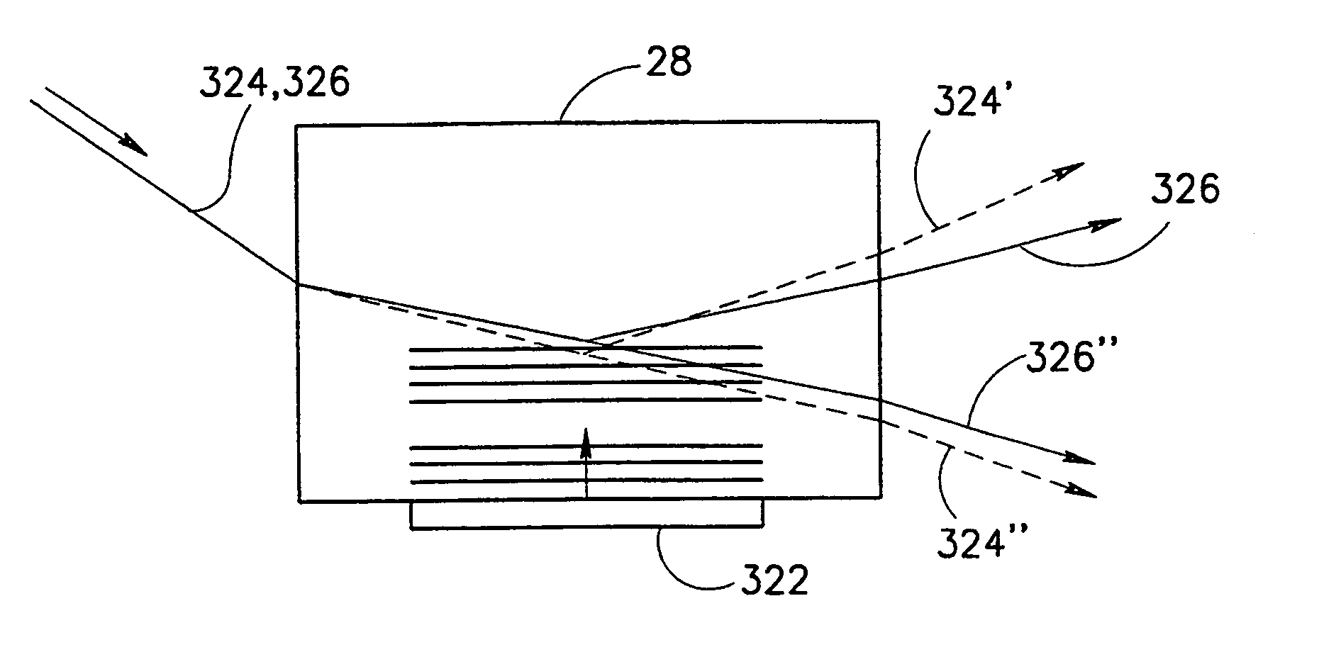
Figure 1 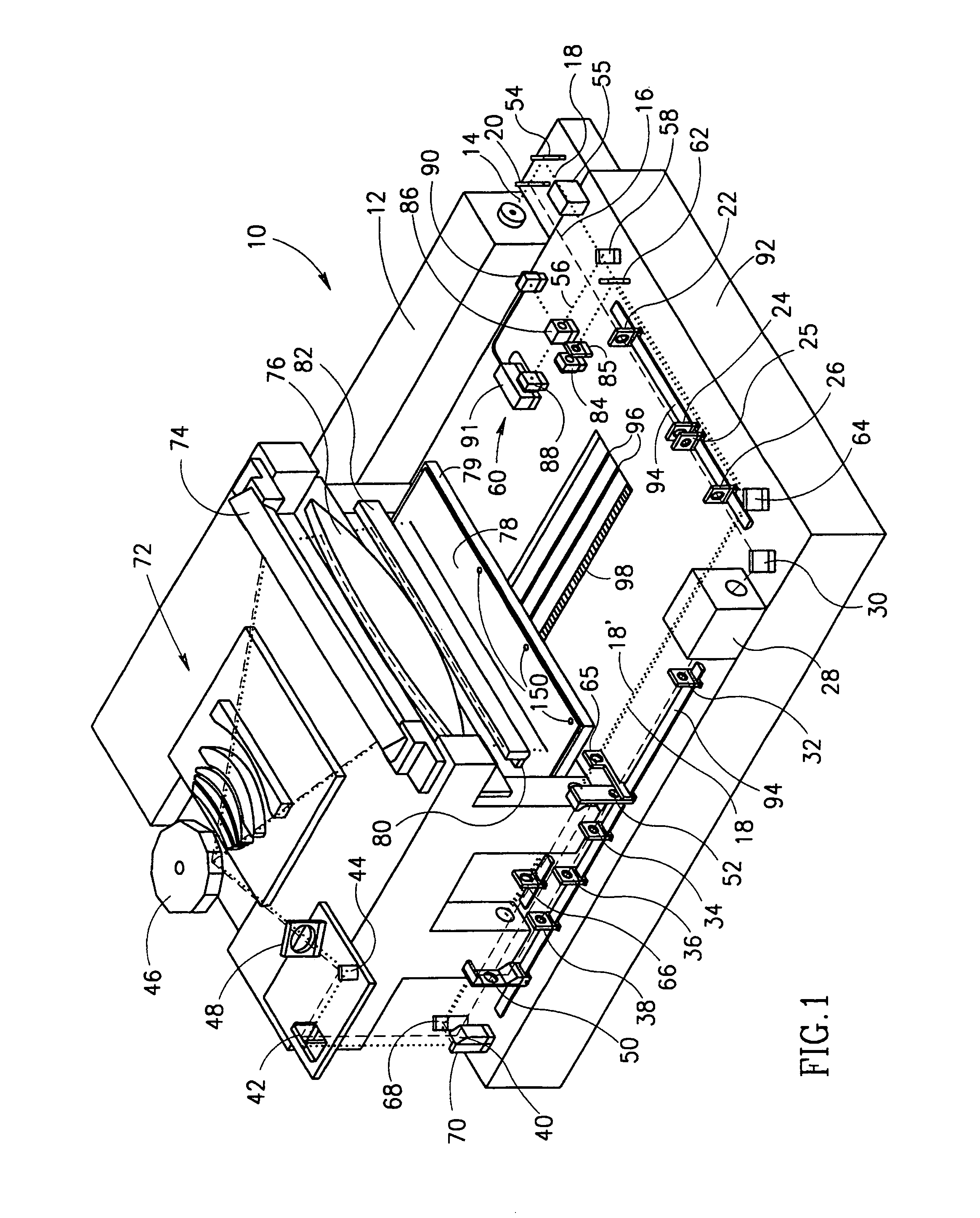
Figure 2 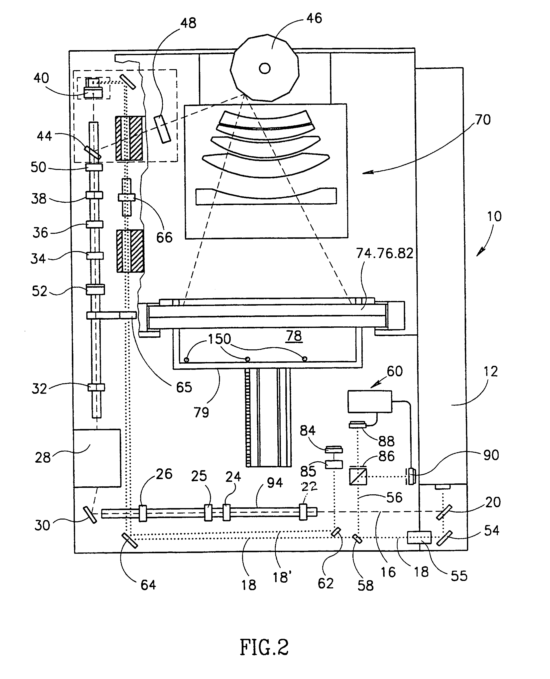
Figure 3
Abstract
Description
RELATED APPLICATION
[0001] This application is the US national stage of PCT Application PCT / EP99 / 01764, filed 15 Mar. 1999.FIELD OF THE INVENTION
[0002] The present invention is related to methods for scanning surfaces, for example for writing on the surfaces with a scanning laser beam. In particular, a system for direct writing of patterns on printed circuit boards is disclosed.BACKGROUND OF THE INVENTION
[0003] Most printed circuit boards are produced by first coating a printed circuit board substrate, having a solid copper cladding, with a photoresist material. When selectively exposed and developed, part of the photoresist is removed and the remaining photoresist forms a pattern corresponding to the light and dark areas of the illumination. After formation of the developed photoresist pattern, the copper cladding is typically subjected to an etching step in which that part of the copper cladding that is not coated by the photoresist is removed.
[0004] In the main, one of two methods of ...
Examples
Embodiment Construction
System Overview
[0185]Reference is made to FIGS. 1–3, which show an exemplary direct writing printed circuit board scanner 10, in accordance with a preferred embodiment of the invention. Scanner 10 comprises a laser source 12, whose output wavelength is suitable for exposing a photoresist coating. In a preferred embodiment of the invention, an Argon Ion type ultraviolet laser, operating at 351.1 and 363.8 nanometers and delivering a maximum power of 4.4 watts has been found suitable. Such lasers are generally available and an Innova Sabre type laser of Coherent, Inc. of California USA or a Beam Lock 2085 type laser of Spectra Physics of California, USA, have both been found suitable. A beam 14 exits source 12 and is split into two beams, a main beam 16 and a test beam 18, by a first beam splitter (or partially reflective mirror) 20. As explained below, main beam 16 (shown as a dashed line), is (eventually) used to scan and expose the photoresist on the printed circuit board. Test bea...