
Optical element module package and method for manufacturing the same
a technology of optical elements and modules, applied in the direction of optical waveguide light guides, semiconductor laser structural details, semiconductor lasers, etc., can solve the problems of increasing manufacturing costs, inconvenient manufacturing procedures, and unsuitable optical element packages for high-speed transmission above several gbps, and achieves simple, reliable and inexpensive implementation.
Patent Information
- Authority / Receiving Office
- US · United States
- Patent Type
- Patents(United States)
- Current Assignee / Owner
- Publication Date
- 2007-01-02
- Estimated Expiration
- Not applicable · inactive patent
Smart Images
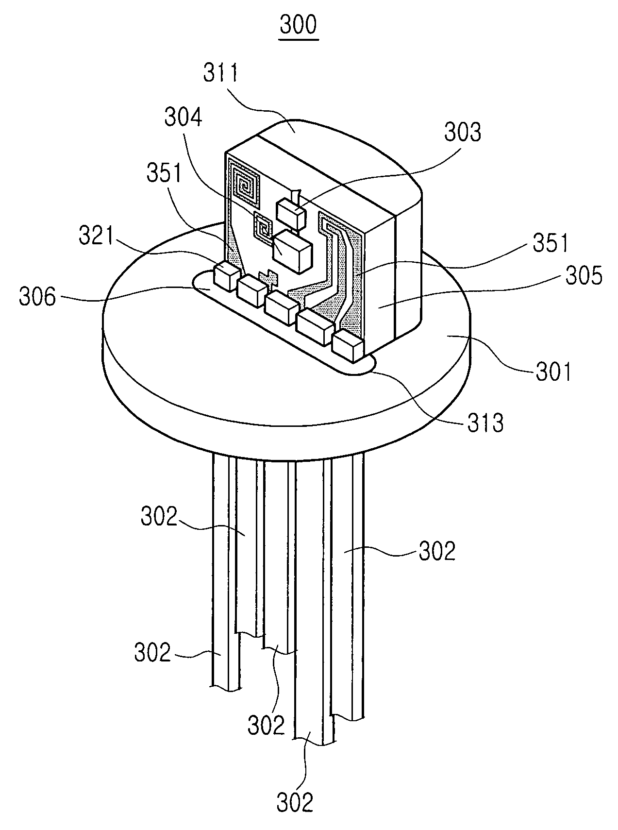
Figure 1 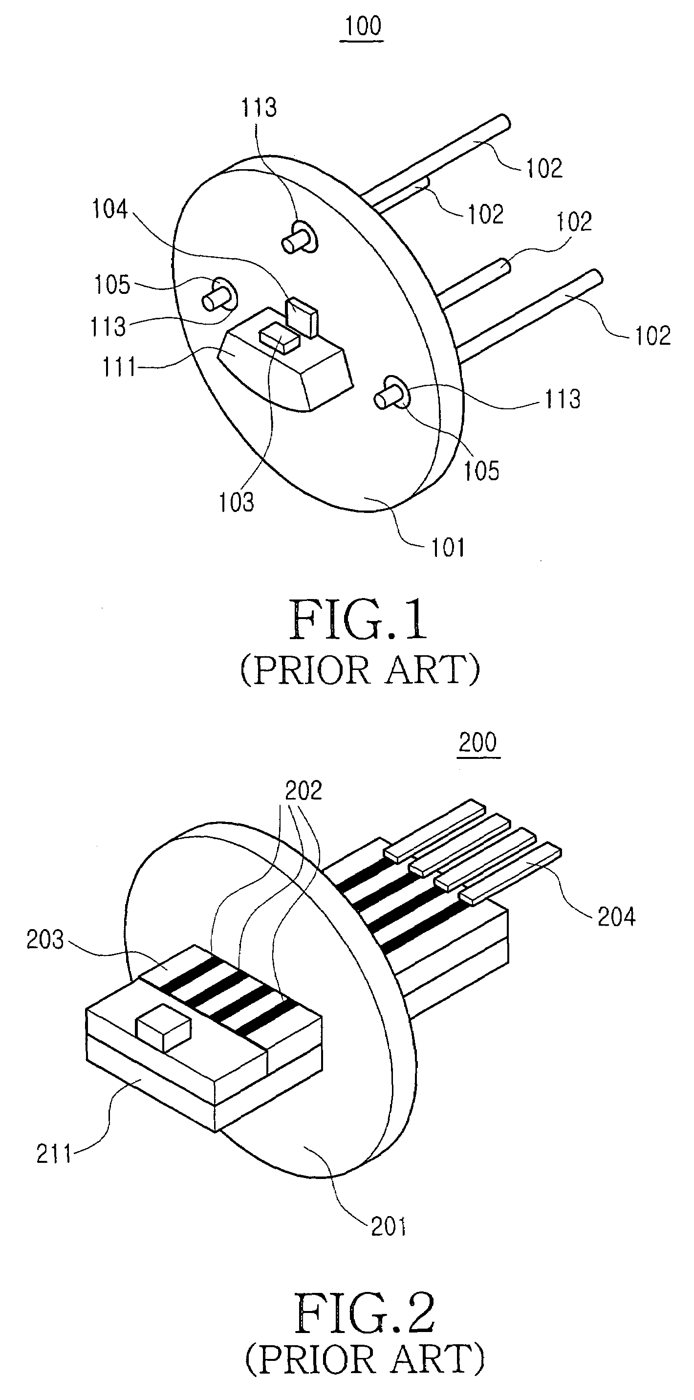
Figure 2 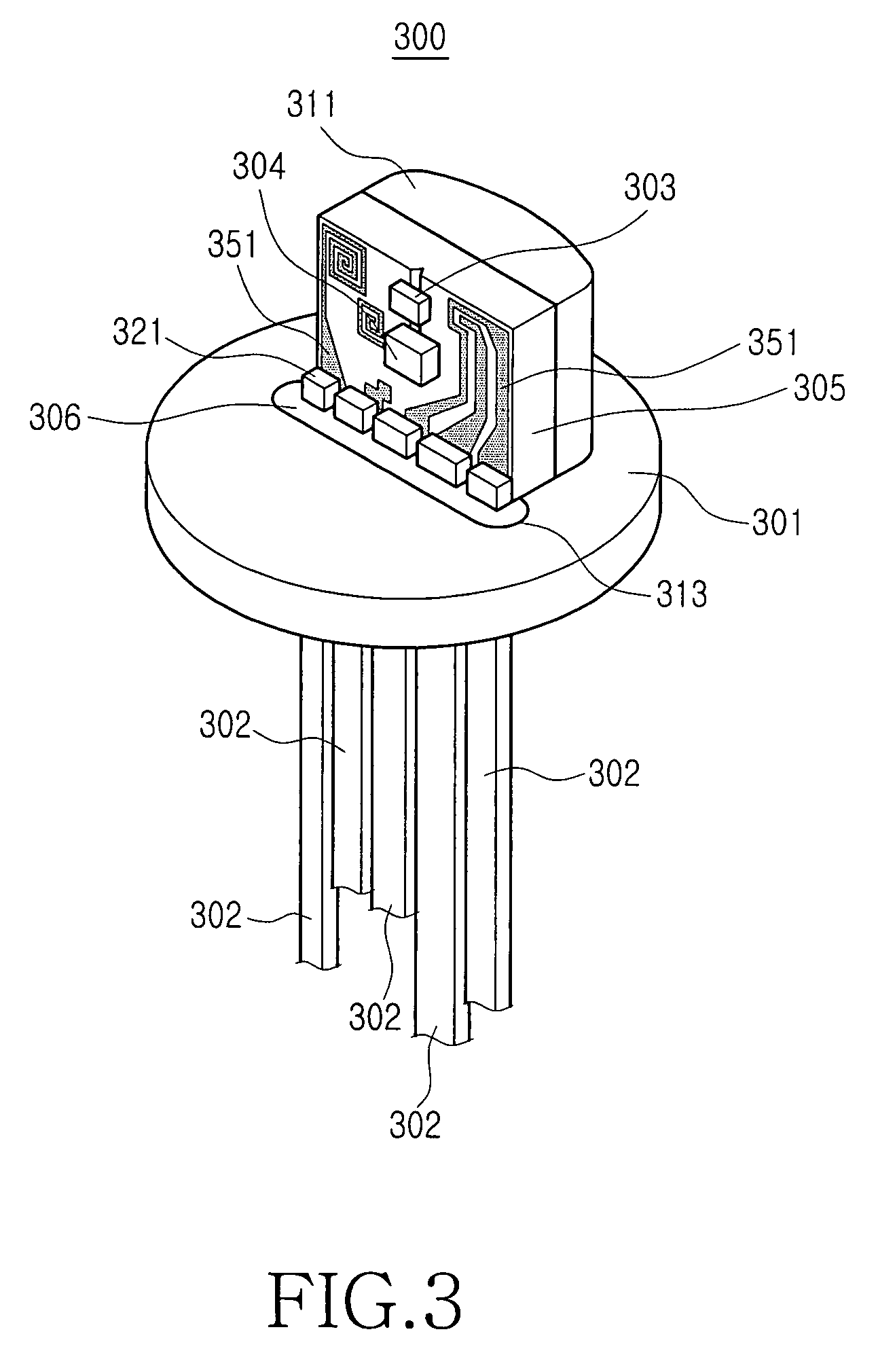
Figure 3
Abstract
Description
CLAIM OF PRIORITY
[0001] This application claims priority to an application entitled “optical element module package and method for manufacturing the same,” filed with the Korean Intellectual Property Office on Jun. 4, 2003 and assigned Serial No. 2003-35965, the contents of which are hereby incorporated by reference.BACKGROUND OF THE INVENTION
[0002] 1. Field of the Invention
[0003] The present invention relates to an optical element module, and more particularly to an optical element module package having a TO-can structure and a method for manufacturing the same.
[0004] 2. Description of the Related Art
[0005] In general, an optical element module, mounted on an electric circuit device (e.g., a printed circuit board), modulates radio-frequency signals into optical signals. Due to a rapid development in the information industry, there is an increasing trend to transmit information by means of an optical communication network as a result of faster and larger data capacity demands. Traditiona...
Examples
Embodiment Construction
[0024]Hereinafter, an optical element module package and a method for manufacturing the same according to preferred embodiments of the present invention will be described with reference to the accompanying drawings. For the purposes of clarity and simplicity, a detailed description of known functions and configurations incorporated herein will be omitted as it may make the subject matter of the present invention unclear.
[0025]As shown in FIGS. 3 to 5, an optical element module package 300 according to a first preferred embodiment of the present invention includes a stem 301 having a heat sink block 311 formed at one end thereof, a sub-mount 305 having a laser diode 303 and a photo diode 304 mounted thereon, and a plurality of leads 302 formed at the other end. In operation, the package 300 projects optical signals when radio-frequency signals are applied to the laser diode 303 and the photo diode 304 mounted on the sub-mount 305.
[0026]The stem 301 has an elongated through-hole 313 e...